Sunday, March 31, 2024

Why L. Ron Hubbard Patented His E-Meter


To call L. Ron Hubbard a prolific writer is an extreme understatement. From 1934 to 1940, he regularly penned 70,000 to 100,000 words per month of pulp fiction under 15 different pseudonyms published in various magazines. Not to be constrained by genre, he wrote zombie mysteries, historical fiction, pirate adventure tales, and westerns.

But by the spring of 1938, Hubbard started honing his craft in science fiction. The publishers of Astounding Science Fiction approached Hubbard to write stories that focused on people, rather than robots and machines. His first story, “The Dangerous Dimension,” was a light-hearted tale about a professor who could teleport anywhere in the universe simply by thinking “Equation C.”

How Scientologists use the E-meter

Twelve years and more than a hundred stories later, Hubbard published a very different essay in the May 1950 issue of Astounding Science Fiction: “Dianetics: The Evolution of a Science.” In the essay, Hubbard recounts his own journey to discover what he called the reactive mind and the “technology” to conquer it. The essay was the companion piece to his simultaneously released book, Dianetics: The Modern Science of Mental Health, which in turn became the foundation for a new religion: the Church of Scientology.

Marrying technology with spirituality, Hubbard introduced the electropsychometer, or E-meter, in the 1950s as a device to help his ministers measure the minds, bodies, and spirits of church members. According to church dogma, the minds of new initiates are impaired by “engrams”—lingering traces of traumas, including those from past lives. An auditor purportedly uses the E-meter to identify and eliminate the engrams, which leads eventually to the person’s reaching a state of being “clear.” Before reaching this desirable state, a church member is known as a “preclear.”

Photo of an electrical device connected by wires to two metal cylinders, a wall plug, and a black object labeled MARK VI. 
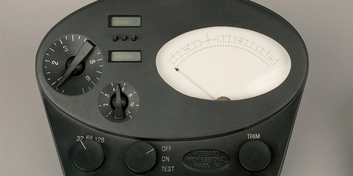
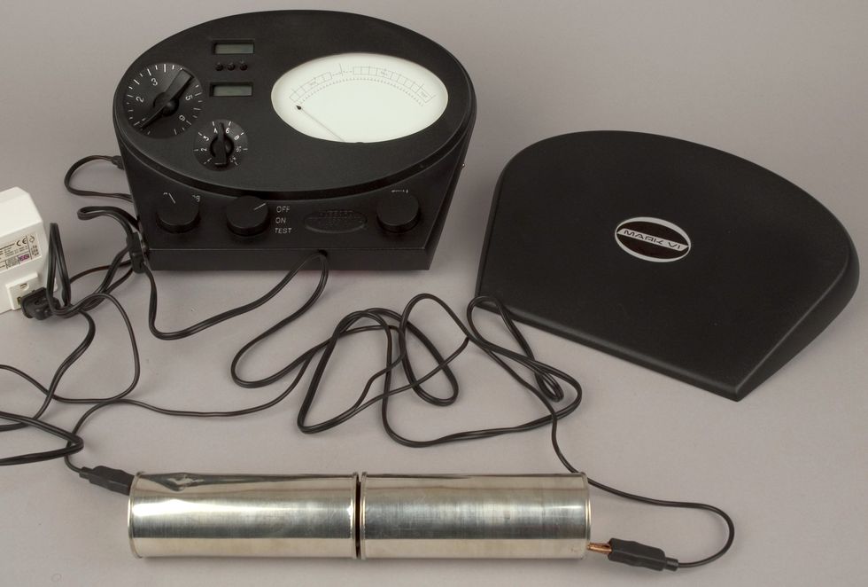
To use the E-meter, a user grasps the metal cylinders while a mild electrical current runs through them. A human auditor interprets the device’s readings.Whipple Museum of the History of Science/University of Cambridge

During an auditing session, a preclear holds the E-meter’s two metal cylinders, one in each hand, as a small electrical current flows through them. The auditor asks a series of questions while operating two dials on the E-meter. The larger dial adjusts the resistance; the smaller dial controls the amplification of the needle. The auditor doesn’t read specific measurements on the meter but rather interprets the needle’s movement as the preclear responds to the questions.

The church’s 2014 Super Bowl ad, which invites viewers to “imagine science and religion connecting,” offers a glamorized glimpse of an auditing session:

Scientology Spiritual Technology - Super Bowl Commercial 2014 youtu.be

In his writings, Hubbard described the E-meter as a Wheatstone bridge, an electrical circuit designed in 1833 by Samuel Hunter Christie to measure an unknown resistance. (Sir Charles Wheatstone popularized the device about a decade later, and his name stuck.) Technically, the E-meter is a modified ohm meter measuring the galvanic skin response of the user—changes in the skin’s electrical resistance, that is. Galvanic skin response is an example of the sympathetic nervous system in action. It’s how your body automatically responds to various stimuli, such as your heart beating faster when you’re scared.

Rejection of L. Ron Hubbard’s claims

Hubbard was not the first to use electrical devices to measure the sympathetic nervous system and consider it a reflection of the mind. As early as 1906, psychologist Carl Jung was noting changes in skin resistance in response to emotionally charged words. By the 1920s, John Larson was using the polygraph to interrogate police subjects.

Hubbard sought approval for his ideas from the medical establishment, but almost immediately, organizations such as the American Psychological Association rejected his theories as pseudoscience. In fact, several scholars looking to dismiss the validity of the E-meter compared it to lie detectors, which also require human operators to interpret the results—and which have also been categorized as being of dubious value by the American Psychological Association and the U.S. National Academy of Sciences.

Black-and-white photo of a white middle-aged man in a suit sitting at a desk. 
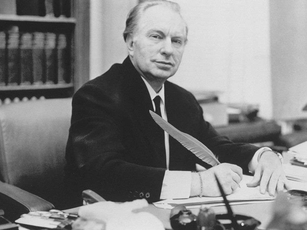
L. Ron Hubbard, shown in 1999, was a prolific sci-fi writer before launching Dianetics and the Church of Scientology.Yves Forestier/Sygma/Getty Images

Government authorities also condemned the church’s claims. In 1951, for example, the New Jersey State Board of Medical Examiners accused one of Hubbard’s foundations of teaching medicine without a license. A few years later, the Food and Drug Administration seized vitamin supplements that Hubbard claimed protected against radiation.

One of the most dramatic episodes occurred in 1963, when U.S. Marshals raided Hubbard’s headquarters in Washington, D.C., and confiscated more than a hundred E-meters. The FDA had issued a warrant that accused the church of falsely claiming that the devices had both physical and mental therapeutic properties. The lawsuit stretched on for years, and the court initially found against the church. On appeal, a judge ruled that the E-meter could be used for religious purposes as long as it clearly displayed this warning label: “The E-Meter is not medically or scientifically useful for the diagnosis, treatment or prevention of disease. It is not medically or scientifically capable of improving the health or bodily functions of anyone.”

Scientologists modified this warning, instead printing this advisory on their instruments: “The Hubbard Electrometer is a religious artifact. By itself, this meter does nothing. It is for religious use by students and ministers of the church in confessionals and pastoral counseling only.”

The E-meter as a recruitment tool

As Scientology spread outside the United States, attacks on the E-meter and the church continued. In Australia, Kevin Anderson wrote the official “Report of the Board of Enquiry Into Scientology” for the state of Victoria. Published in 1965, it became known as the Anderson Report. He did not mince words: “Scientology is evil; its techniques evil; its practice a serious threat to the community, medically, morally and socially; and its adherents sadly deluded and often mentally ill.”

Photo of a man in a suit demonstrating an electrical device to small children. In 1961, Hubbard wrote of his recent discovery that the E-meter requires the auditor to have “command value” over the person being audited.Keystone Press/Alamy

Chapter 14 of the report is devoted to the E-meter, which Anderson viewed as a powerful enabler of Scientology. After describing its construction and use, the report offers expert witness testimony negating Scientologists’ claims, based on the modern understanding of electrical resistance. It then points out specific claims that stretch credulity, such as how the E-meter supposedly helps preclears recall incidents trillions of years in the past down to the precise second. The report quotes from Hubbard’s written recollection of having received an implant “43,891,832,611,177 years, 344 days, 10 hours, 20 minutes and 40 seconds from 10:02.30 P.M. Daylight Greenwich Time May 9, 1963.”

The report also cites the Hubbard Communications Office Bulletin of 30 November 1961, in which Hubbard admits: “An E-meter has a frailty I have just discovered. It operates only if the auditor has some, even small, command value over the pc [preclear], and operates hardly at all when the auditor has no command value over the pc.” Given this imbalance between the auditor and the preclear, Anderson reasoned, the E-meter is a powerful tool for manipulation. “Fears of its abilities keep [preclears] in constant subjection,” the report states. “Its use can be so manipulated by cunningly phrased questions that almost any desired result can be obtained, and it is used unscrupulously to dominate students and staff alike. All the evil features of scientology are intensified where the E-meter is involved.”

Hubbard’s response? The report was simply a kangaroo court that already knew its conclusions before the first witness was called.

The E-meter patents never mentioned religion

Although Hubbard didn’t invent the E-meter, he inspired its creation, came up with a transistorized, battery-powered unit, and received several patents for later versions.

In his patents (see, for example, U.S. Patent No. 3,290,589, “Device for Measuring and Indicating Changes in Resistance of a Living Body”), Hubbard stuck to technical descriptions of the circuitry. The patents made no claims about reading a person’s thoughts or using the device for religious purposes. But Hubbard’s own writings are chock-full of technobabble, intermingling actual technical terms with statements that are demonstrably false. One of my favorites is his differentiation of the resistances of dead male and female bodies: 12,500 ohms and 5,000 ohms, respectively.

Obviously, from the viewpoint of contemporary science, the claims that the E-meter unlocks past-life traumas cannot be verified or replicated. The instruments themselves are imprecise and unreliable, the readouts depending on things like how the cylinders are grasped. And of course, the auditor can interpret the results any way they choose. Scientists and psychologists routinely denounce Scientology as quackery, yet at the same time, religious scholars find parallels to older, well-established faiths.

Centuries ago, Copernicus and Galileo posited a new science that flew in the face of religious beliefs. L. Ron Hubbard turned that idea on its head and founded a new religion purportedly based on science, and he positioned the E-meter as the device for entangling technology and spirituality.

Part of a continuing series looking at historical artifacts that embrace the boundless potential of technology.

An abridged version of this article appears in the April 2024 print issue as “The Scientology Machine.”

References


In researching the E-meter, I quickly found the literature to be polarizing, divided among the true believers, those set to debunk the science, and scholars trying to make sense of it all.

L. Ron Hubbard was a prolific writer as well as a lecturer, and so there are tons of primary sources. I found Introducing the E-meter to be a great starting place.

David S. Touretzky, a computer science professor at Carnegie Mellon University, maintains an extensive website critiquing the E-meter. He includes numerous Scientology texts, along with his own explanations.

Stefano Bigliardi’s article “New Religious Movements, Technology, and Science: The Conceptualization of the E-meter in Scientology Teachings,” in Zygon: Journal of Religion and Science (September 2016), offered an even-handed discussion of the E-meter, reflecting on its function and symbolic meaning within various Scientology texts.

Reference: https://ift.tt/G9oU7bk

Friday, March 29, 2024

Playboy image from 1972 gets ban from IEEE computer journals


Playboy image from 1972 gets ban from IEEE computer journals

Enlarge (credit: Aurich Lawson | Getty Image)

On Wednesday, the IEEE Computer Society announced to members that, after April 1, it would no longer accept papers that include a frequently used image of a 1972 Playboy model named Lena Forsén. The so-called "Lenna image," (Forsén added an extra "n" to her name in her Playboy appearance to aid pronunciation) has been used in image processing research since 1973 and has attracted criticism for making some women feel unwelcome in the field.

In an email from the IEEE Computer Society sent to members on Wednesday, Technical & Conference Activities Vice President Terry Benzel wrote, "IEEE's diversity statement and supporting policies such as the IEEE Code of Ethics speak to IEEE's commitment to promoting an including and equitable culture that welcomes all. In alignment with this culture and with respect to the wishes of the subject of the image, Lena Forsén, IEEE will no longer accept submitted papers which include the 'Lena image.'"

An uncropped version of the 512×512-pixel test image originally appeared as the centerfold picture for the December 1972 issue of Playboy Magazine. Usage of the Lenna image in image processing began in June or July 1973 when an assistant professor named Alexander Sawchuck and a graduate student at the University of Southern California Signal and Image Processing Institute scanned a square portion of the centerfold image with a primitive drum scanner, omitting nudity present in the original image. They scanned it for a colleague's conference paper, and after that, others began to use the image as well.

Read 6 remaining paragraphs | Comments

Reference : https://ift.tt/xEYV4se

Fusion Tech Finds Geothermal Energy Application


The upper 10 kilometers of the Earth’s crust contains vast geothermal reserves, essentially awaiting human energy consumption to begin to tap into its unstinting power output—which itself yields no greenhouse gasses. And yet, geothermal sources currently produce only three-tenths of one percent of the world’s electricity. This promising energy source has long been limited by the extraordinary challenges of drilling holes that are deep enough to access the intense heat below the Earth’s surface.

Now, an MIT spin-off says it has found a solution in an innovative technology that could dramatically reduce the costs and timelines of drilling to fantastic depths. Quaise Energy, based in Cambridge, Mass., plans to deploy what are called gyroton drills to vaporize rock using powerful microwaves.

“We need to go deeper and hotter to make geothermal energy viable outside of places like Iceland.” —Carlos Araque, Quaise Energy

A gyrotron uses high-power, linear-beam vacuum tubes to generate millimeter-length electromagnetic waves. Invented by Soviet scientists in the 1960s, gyrotons are used in nuclear fusion research experiments to heat and control plasma. Quaise has raised $95 million from investors, including Japan’s Mitsubishi, to develop technology that would enable it to quickly and efficiently drill up 20 km deep, closer to the Earth’s core than ever before.

photo of metal cylindrical chamber with pipes and hoses and dials attached Quaise Energy has developed a prototype portable gyrotron, which they plan to be conducting field tests with later this year.Quaise Energy

“Supercritical geothermal power has the potential to replace fossil fuels and finally give us a pathway to an energy transition to carbon-free, baseload energy,” says Quaise CEO Carlos Araque, a veteran of the oil and gas industry and former technical director of The Engine Accelerator, MIT’s platform to commercialize world-changing technologies. “We need to go deeper and hotter to make geothermal energy viable outside of places like Iceland.”

The deepest man-made hole, which extends 12,262 meters below the surface of Siberia, took nearly 20 years to drill. As the shaft went deeper, progress declined to less than a meter per hour—a rate that finally decreased to zero as the work was abandoned in 1992. That attempt and similar projects have made it clear that conventional drills are no match for the high temperatures and pressures deep in the Earth’s crust.

Microwaves meet rocks

“But an energy beam doesn’t have those kinds of limits,” says Paul Woskov, senior research engineer at MIT’s Plasma Science and Fusion Center. Woskov spent decades working with powerful microwave beams, steering them into precise locations to heat hydrogen fuel above 100 million degrees to initiate fusion reactions.

“It wasn’t much of a jump to make the connection that if we can melt steel chambers and vaporize them, we could melt rocks.” —Paul Woskov, MIT

“I was already aware that these sources were quite damaging to materials because one of the challenges is not to melt the inner chamber of a tokamak,” a device that confines a plasma using magnetic fields. “So it wasn’t much of a jump to make the connection that if we can melt steel chambers and vaporize them, we could melt rocks.”

In 2008, Woskov began intensively studying whether the approach could be an affordable improvement on mechanical drilling. The research led to hands-on experiments in which Woskov used a small gyrotron to blast through bricks of basalt.

Based on his experiments and other research, Woskov calculated that a millimeter-wave source targeted through a roughly 20 centimeter waveguide could blast a basketball-size hole into rock at a rate of 20 meters per hour. At that rate, 25-and-a-half days of continuous drilling would create the world’s deepest hole.

“It was evident that if we could get it to work, we could drill very deep holes for a very small fraction of what it costs now,” says Wostov. Although Wostov is credited as a founder of Quaise, he says he has no financial stake in the company—unlike MIT.

A wave of possibilities

The Quaise design calls for a corrugated metal tube to serve as a waveguide, which would be extracted after drilling is completed. The system would rely on injected gas to quench and carry out ash.

“Instead of pumping fluid and turning a drill, we’ll be burning and vaporizing rock and extracting gas, which is much easier to pump than mud.” —Carlos Araque, Quaise Energy

“We will need about a megawatt to power it, the same amount of energy as a typical drilling rig,” says Araque. ”But we’ll be using it in very different ways. Instead of pumping fluid and turning a drill, we’ll be burning and vaporizing rock and extracting gas, which is much easier to pump than mud.”

Using the waveguide to direct energy to the targeted rock allows the energy source to stay on the surface. That may sound like a stretch, but the concept was tested in a 1970s experiment in which Bell Labs built a 14 km waveguide transmission medium in northern New Jersey. The researchers found that it could transmit millimeter waves with very little attenuation.

Quaise intends to first target industrial customers with a need for steam at a guaranteed flow rate, temperature, and pressure. “Our goal is to match the specs of an industrial load,” says Araque. “They can retire the boiler, and we’ll give them 500º C steam on-site.”

Eventually, the company hopes the technology could enable new geothermal electric plants, or allow turbines formerly heated by fossil fuels to be repurposed—supplying the grid with an estimated 25-50 megawatts of electricity from each well.

The company plans to begin field demonstrations this autumn, using a prototype device to drill holes in hard rock at a site in Marble Falls, Tex. From there, Quaise plans to build a full-size demonstration rig in a high-geothermal zone in the western United States.

Image of a rock surface with a melted hole in the middle that appears to extend deep into the rock surface 
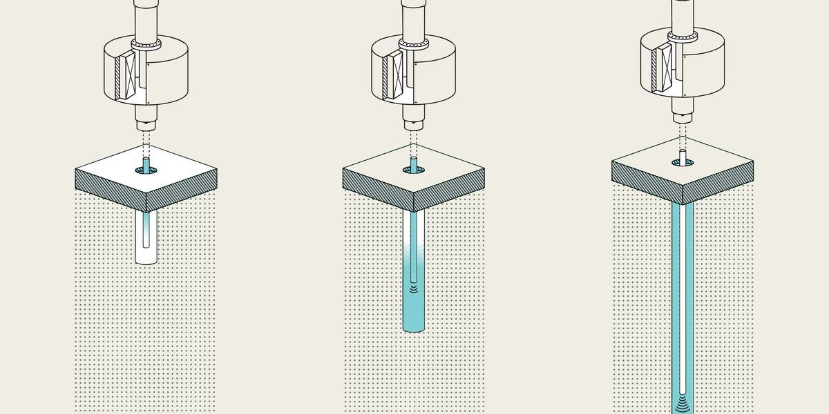
Quaise Energy drilled a hole 254 centimeters (100 inches) deep with a 2.5 cm diameter into a column of basalt, making it 100 times the depth of the team’s original tests, as conducted at MIT.Quaise Energy

Facing the depths

Although laboratory data have demonstrated the feasibility of scaling up the approach, the technical obstacles to the Quaise plan are likely to run deeper than its radical drilling method.

“If they can actually drill a 10 km hole using high-powered microwaves, that will be a significant engineering achievement,” says Jefferson Tester, who studies geothermal energy extraction in subsurface rock reservoirs at Cornell University. “But the challenge is completing those wells so they don’t fall apart, particularly if you’re going to start removing fluids from underground and changing the temperature profile.

“Drilling a hole is challenging enough,” says Tester. “But actually running the reservoir and getting the energy out of the ground safely may be something very, very far off in the future.”

Reference: https://ift.tt/8in4Bma

Backdoor found in widely used Linux utility breaks encrypted SSH connections


Internet Backdoor in a string of binary code in a shape of an eye.

Enlarge / Internet Backdoor in a string of binary code in a shape of an eye. (credit: Getty Images)

Researchers have found a malicious backdoor in a compression tool that made its way into widely used Linux distributions, including those from Red Hat and Debian.

The compression utility, known as xz Utils, introduced the malicious code in versions ​​5.6.0 and 5.6.1, according to Andres Freund, the developer who discovered it. There are no confirmed reports of those versions being incorporated into any production releases for major Linux distributions, but both Red Hat and Debian reported that recently published beta releases used at least one of the backdoored versions—specifically, in Fedora 40 and Fedora Rawhide and Debian testing, unstable and experimental distributions.

Because the backdoor was discovered before the malicious versions of xz Utils were added to production versions of Linux, “it's not really affecting anyone in the real world,” Will Dormann, a senior vulnerability analyst at security firm ANALYGENCE, said in an online interview. “BUT that's only because it was discovered early due to bad actor sloppiness. Had it not been discovered, it would have been catastrophic to the world.”

Read 9 remaining paragraphs | Comments

Reference : https://ift.tt/Zkfi2LY

OpenAI holds back wide release of voice-cloning tech due to misuse concerns


AI speaks letters, text-to-speech or TTS, text-to-voice, speech synthesis applications, generative Artificial Intelligence, futuristic technology in language and communication.

Enlarge (credit: Getty Images)

Voice synthesis has come a long way since 1978's Speak & Spell toy, which once wowed people with its state-of-the-art ability to read words aloud using an electronic voice. Now, using deep-learning AI models, software can create not only realistic-sounding voices, but also convincingly imitate existing voices using small samples of audio.

Along those lines, OpenAI just announced Voice Engine, a text-to-speech AI model for creating synthetic voices based on a 15-second segment of recorded audio. It has provided audio samples of the Voice Engine in action on its website.

Once a voice is cloned, a user can input text into the Voice Engine and get an AI-generated voice result. But OpenAI is not ready to widely release its technology yet. The company initially planned to launch a pilot program for developers to sign up for the Voice Engine API earlier this month. But after more consideration about ethical implications, the company decided to scale back its ambitions for now.

Read 14 remaining paragraphs | Comments

Reference : https://ift.tt/JktoxaL

Thursday, March 28, 2024

Salt-Sized Sensors Mimic the Brain


To gain a better understanding of the brain, why not draw inspiration from it? At least, that’s what researchers at Brown University did, by building a wireless communications system that mimics the brain using an array of tiny silicon sensors, each the size of a grain of sand. The researchers hope that the technology could one day be used in implantable brain-machine interfaces to read brain activity.

Each sensor, measuring 300 by 300 micrometers, acts as a wireless node in a large array, analogous to neurons in the brain. When a node senses an event, such as a change in temperature or neural activity, the device sends the data as a “spike” signal, consisting of a series of short radiofrequency pulses, to a central receiver. That receiver then decodes the information.

“The brain is exquisitely efficient in handling large amounts of data,” says Arto Nurmikko, a professor of engineering and physics at Brown University. That’s why his lab chose to develop a network of unobtrusive microsensors that are “neuromorphic,” meaning they are inspired by how the brain works. And the similarities don’t end there—Nurmikko says that the wireless signals and computing methods are also inspired by the brain. The team published their results on 19 March in Nature Electronics.

Thinking Like a Brain

Like neurons, these sensors are event-driven and only send signals to the receiver when a change occurs. While digital communication encodes information in a sequence of ones and zeros, this system cuts down the amount of data transmitted by using periods of inactivity to infer where zeros would be sent. Importantly, this leads to significant energy savings, which in turn allows for a larger collection of microsensors.

But with so many sensors sending information to a common receiver, it can be difficult to keep the data streams straight. The researchers deployed a neuromorphic computing technique to decode the signals in real time.

“The brain is exquisitely efficient in handling large amounts of data.” —Arto Nurmikko, Brown University

The researchers also conducted simulations to test the system’s error rate, which increases with more sensors. In addition to 78 fabricated sensors, they ran simulations of networks consisting of 200, 500, and 1,000 nodes using a real data set from primate brain recordings. In each, the system predicted the hand movement of a non-human primate with an error rate below 0.1 percent, which is acceptable for brain-computer applications. Nurmikko says the team will next test the wireless implanted sensor network in rodents.

While the technology could be applied to any part of the body where biomedical researchers aim to monitor physiological activity, the primary goal is use in a brain-machine interface that can probe a large region of the brain, says Nurmikko. The sensors could also be modified for use in wearable technology or environmental sensors.

There are key advantages of the system for biomedical uses, such as the small, unobtrusive design. But these applications also impose a key limitation: The sensors are externally powered by a wireless beam to avoid the need for batteries, and the body can only safely absorb so much radiofrequency energy. In other words, the system is not limited by bandwidth, but instead by power delivery. “From a practical point of view, it always comes back to the question of, where do you get your energy?” says Nurmikko.

Brain-Machine Interface Possibilities

The research provides “an important contribution, which demonstrates the feasibility and potential of neuromorphic communications for future use cases of low-power wireless sensing, communication, and decision making,” says Osvaldo Simeone, a professor at King’s College London and one of the researchers who first designed and simulated a neuromorphic communication system in 2020.

The idea of a wireless network probing the brain is not new, says Federico Corradi, a researcher and assistant professor of electrical engineering at Eindhoven University of Technology. In 2011, for example, a researcher at UC Berkeley gave a presentation on “neural dust” in which he proposed a hypothetical class of nanometer-sized wireless sensors. “But now, it’s materializing slowly,” Corradi says.

One important element of the Brown researcher’s design is its simplicity, says Corradi. The sensor’s architecture does not include a battery or clock embedded within the chips, making it ideal for scalable, low-power systems. “It opens a lot of possibilities.”

Additionally, Corradi points to the sensor’s asynchronous nature as a key advantage—and limitation. This aspect of the sensor preserves time information, which is essential for studying the brain. But this feature could also introduce problems if the relative timing of events gets out of whack.

Corradi believes this work is part of a larger trend toward neuromorphic systems, a “new wave of brain-machine interfaces that I hope we will see in the coming future.”

Reference: https://ift.tt/sBCfS9O

How We’ll Reach a 1 Trillion Transistor GPU


In 1997 the IBM Deep Blue supercomputer defeated world chess champion Garry Kasparov. It was a groundbreaking demonstration of supercomputer technology and a first glimpse into how high-performance computing might one day overtake human-level intelligence. In the 10 years that followed, we began to use artificial intelligence for many practical tasks, such as facial recognition, language translation, and recommending movies and merchandise.

Fast-forward another decade and a half and artificial intelligence has advanced to the point where it can “synthesize knowledge.” Generative AI, such as ChatGPT and Stable Diffusion, can compose poems, create artwork, diagnose disease, write summary reports and computer code, and even design integrated circuits that rival those made by humans.

Tremendous opportunities lie ahead for artificial intelligence to become a digital assistant to all human endeavors. ChatGPT is a good example of how AI has democratized the use of high-performance computing, providing benefits to every individual in society.

All those marvelous AI applications have been due to three factors: innovations in efficient machine-learning algorithms, the availability of massive amounts of data on which to train neural networks, and progress in energy-efficient computing through the advancement of semiconductor technology. This last contribution to the generative AI revolution has received less than its fair share of credit, despite its ubiquity.

Over the last three decades, the major milestones in AI were all enabled by the leading-edge semiconductor technology of the time and would have been impossible without it. Deep Blue was implemented with a mix of 0.6- and 0.35-micrometer-node chip-manufacturing technology. The deep neural network that won the ImageNet competition, kicking off the current era of machine learning, was implemented with 40-nanometer technology. AlphaGo conquered the game of Go using 28-nm technology, and the initial version of ChatGPT was trained on computers built with 5-nm technology. The most recent incarnation of ChatGPT is powered by servers using even more advanced 4-nm technology. Each layer of the computer systems involved, from software and algorithms down to the architecture, circuit design, and device technology, acts as a multiplier for the performance of AI. But it’s fair to say that the foundational transistor-device technology is what has enabled the advancement of the layers above.

If the AI revolution is to continue at its current pace, it’s going to need even more from the semiconductor industry. Within a decade, it will need a 1-trillion-transistor GPU—that is, a GPU with 10 times as many devices as is typical today.

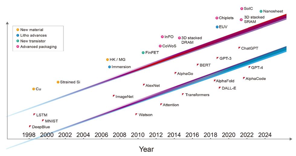
Advances in semiconductor technology [top line]—including new materials, advances in lithography, new types of transistors, and advanced packaging—have driven the development of more capable AI systems [bottom line]

Relentless Growth in AI Model Sizes

The computation and memory access required for AI training have increased by orders of magnitude in the past five years. Training GPT-3, for example, requires the equivalent of more than 5 billion billion operations per second of computation for an entire day (that’s 5,000 petaflops-days), and 3 trillion bytes (3 terabytes) of memory capacity.

Both the computing power and the memory access needed for new generative AI applications continue to grow rapidly. We now need to answer a pressing question: How can semiconductor technology keep pace?

From Integrated Devices to Integrated Chiplets

Since the invention of the integrated circuit, semiconductor technology has been about scaling down in feature size so that we can cram more transistors into a thumbnail-size chip. Today, integration has risen one level higher; we are going beyond 2D scaling into 3D system integration. We are now putting together many chips into a tightly integrated, massively interconnected system. This is a paradigm shift in semiconductor-technology integration.

In the era of AI, the capability of a system is directly proportional to the number of transistors integrated into that system. One of the main limitations is that lithographic chipmaking tools have been designed to make ICs of no more than about 800 square millimeters, what’s called the reticle limit. But we can now extend the size of the integrated system beyond lithography’s reticle limit. By attaching several chips onto a larger interposer—a piece of silicon into which interconnects are built—we can integrate a system that contains a much larger number of devices than what is possible on a single chip. For example, TSMC’s chip-on-wafer-on-substrate (CoWoS) technology can accommodate up to six reticle fields’ worth of compute chips, along with a dozen high-bandwidth-memory (HBM) chips.

How Nvidia Uses CoWoS Advanced Packaging


CoWoS, TSMC’s chip-on-wafer-on-silicon advanced packaging technology, has already been deployed in products. Examples include the Nvidia Ampere and Hopper GPUs. Each consists of one GPU die with six high-bandwidth memory cubes all on a silicon interposer. The compute GPU die is about as large as chipmaking tools will currently allow. Ampere has 54 billion transistors, and Hopper has 80 billion. The transition from 7-nm technology to the denser 4-nm technology made it possible to pack 50 percent more transistors on essentially the same area. Ampere and Hopper are the workhorses for today’s large language model (LLM) training. It takes tens of thousands of these processors to train ChatGPT.


HBMs are an example of the other key semiconductor technology that is increasingly important for AI: the ability to integrate systems by stacking chips atop one another, what we at TSMC call system-on-integrated-chips (SoIC). An HBM consists of a stack of vertically interconnected chips of DRAM atop a control logic IC. It uses vertical interconnects called through-silicon-vias (TSVs) to get signals through each chip and solder bumps to form the connections between the memory chips. Today, high-performance GPUs use HBM extensively.

Going forward, 3D SoIC technology can provide a “bumpless alternative” to the conventional HBM technology of today, delivering far denser vertical interconnection between the stacked chips. Recent advances have shown HBM test structures with 12 layers of chips stacked using hybrid bonding, a copper-to-copper connection with a higher density than solder bumps can provide. Bonded at low temperature on top of a larger base logic chip, this memory system has a total thickness of just 600 µm.

With a high-performance computing system composed of a large number of dies running large AI models, high-speed wired communication may quickly limit the computation speed. Today, optical interconnects are already being used to connect server racks in data centers. We will soon need optical interfaces based on silicon photonics that are packaged together with GPUs and CPUs. This will allow the scaling up of energy- and area-efficient bandwidths for direct, optical GPU-to-GPU communication, such that hundreds of servers can behave as a single giant GPU with a unified memory. Because of the demand from AI applications, silicon photonics will become one of the semiconductor industry’s most important enabling technologies.

Toward a Trillion Transistor GPU

How AMD Uses 3D Technology


The AMD MI300A Accelerated Processor Unit leverages not just CoWoS but also TSMC’s 3D technology, silicon-on-integrated-circuits (SoIC). The MI300A combines GPU and CPU cores designed to handle the largest AI workloads. The GPU performs the intensive matrix multiplication operations for AI, while the CPU controls the operations of the entire system, and the high-bandwidth memories (HBM) are unified to serve both. The 9 compute dies built with 5-nm technology are stacked on top of 4 base dies of 6-nm technology, which are dedicated to cache and I/O traffic. The base dies and HBM sit atop silicon interposers. The compute part of the processor is composed of 150 billion transistors.


As noted already, typical GPU chips used for AI training have already reached the reticle field limit. And their transistor count is about 100 billion devices. The continuation of the trend of increasing transistor count will require multiple chips, interconnected with 2.5D or 3D integration, to perform the computation. The integration of multiple chips, either by CoWoS or SoIC and related advanced packaging technologies, allows for a much larger total transistor count per system than can be squeezed into a single chip. We forecast that within a decade a multichiplet GPU will have more than 1 trillion transistors.

We’ll need to link all these chiplets together in a 3D stack, but fortunately, industry has been able to rapidly scale down the pitch of vertical interconnects, increasing the density of connections. And there is plenty of room for more. We see no reason why the interconnect density can’t grow by an order of magnitude, and even beyond.

Toward a Trillion Transistors


Vertical connection density in 3D chips has increased at roughly the same rate as the number of transistors in a GPU.


Energy-Efficient Performance Trend for GPUs

So, how do all these innovative hardware technologies contribute to the performance of a system?

We can see the trend already in server GPUs if we look at the steady improvement in a metric called energy-efficient performance. EEP is a combined measure of the energy efficiency and speed of a system. Over the past 15 years, the semiconductor industry has increased energy-efficient performance about threefold every two years. We believe this trend will continue at historical rates. It will be driven by innovations from many sources, including new materials, device and integration technology, extreme ultraviolet (EUV) lithography, circuit design, system architecture design, and the co-optimization of all these technology elements, among other things.


Largely thanks to advances in semiconductor technology, a measure called energy-efficient performance is on track to triple every two years (EEP units are 1/femtojoule-picoseconds).


In particular, the EEP increase will be enabled by the advanced packaging technologies we’ve been discussing here. Additionally, concepts such as system-technology co-optimization (STCO), where the different functional parts of a GPU are separated onto their own chiplets and built using the best performing and most economical technologies for each, will become increasingly critical.

A Mead-Conway Moment for 3D Integrated Circuits

In 1978, Carver Mead, a professor at the California Institute of Technology, and Lynn Conway at Xerox PARC invented a computer-aided design method for integrated circuits. They used a set of design rules to describe chip scaling so that engineers could easily design very-large-scale integration (VLSI) circuits without much knowledge of process technology.

That same sort of capability is needed for 3D chip design. Today, designers need to know chip design, system-architecture design, and hardware and software optimization. Manufacturers need to know chip technology, 3D IC technology, and advanced packaging technology. As we did in 1978, we again need a common language to describe these technologies in a way that electronic design tools understand. Such a hardware description language gives designers a free hand to work on a 3D IC system design, regardless of the underlying technology. It’s on the way: An open-source standard, called 3Dblox, has already been embraced by most of today’s technology companies and electronic design automation (EDA) companies.

The Future Beyond the Tunnel

In the era of artificial intelligence, semiconductor technology is a key enabler for new AI capabilities and applications. A new GPU is no longer restricted by the standard sizes and form factors of the past. New semiconductor technology is no longer limited to scaling down the next-generation transistors on a two-dimensional plane. An integrated AI system can be composed of as many energy-efficient transistors as is practical, an efficient system architecture for specialized compute workloads, and an optimized relationship between software and hardware.

For the past 50 years, semiconductor-technology development has felt like walking inside a tunnel. The road ahead was clear, as there was a well-defined path. And everyone knew what needed to be done: shrink the transistor.

Now, we have reached the end of the tunnel. From here, semiconductor technology will get harder to develop. Yet, beyond the tunnel, many more possibilities lie ahead. We are no longer bound by the confines of the past.

Reference: https://ift.tt/lIxVkyW

Wednesday, March 27, 2024

Thousands of servers hacked in ongoing attack targeting Ray AI framework


Thousands of servers hacked in ongoing attack targeting Ray AI framework

Enlarge (credit: Getty Images)

Thousands of servers storing AI workloads and network credentials have been hacked in an ongoing attack campaign targeting a reported vulnerability in Ray, a computing framework used by OpenAI, Uber, and Amazon.

The attacks, which have been active for at least seven months, have led to the tampering of AI models. They have also resulted in the compromise of network credentials, allowing access to internal networks and databases and tokens for accessing accounts on platforms including OpenAI, Hugging Face, Stripe, and Azure. Besides corrupting models and stealing credentials, attackers behind the campaign have installed cryptocurrency miners on compromised infrastructure, which typically provides massive amounts of computing power. Attackers have also installed reverse shells, which are text-based interfaces for remotely controlling servers.

Hitting the jackpot

“When attackers get their hands on a Ray production cluster, it is a jackpot,” researchers from Oligo, the security firm that spotted the attacks, wrote in a post. “Valuable company data plus remote code execution makes it easy to monetize attacks—all while remaining in the shadows, totally undetected (and, with static security tools, undetectable).”

Read 12 remaining paragraphs | Comments

Reference : https://ift.tt/xGMprDe

Canva’s Affinity acquisition is a non-subscription-based weapon against Adobe


Affinity's photo editor.

Enlarge / Affinity's photo editor. (credit: Canva)

Online graphic design platform provider Canva announced its acquisition of Affinity on Tuesday. The purchase adds tools for creative professionals to the Australian startup's repertoire, presenting competition for today's digital design stronghold, Adobe.

The companies didn't provide specifics about the deal, but Cliff Obrecht, Canva's co-founder and COO, told Bloomberg that it consists of cash and stock and is worth "several hundred million pounds."

Canva, which debuted in 2013, has made numerous acquisitions to date, including Flourish, Kaleido, and Pixabay, but its purchase of Affinity is its biggest yet—by both price and headcount (90). Affinity CEO Ashley Hewson said via a YouTube video that Canva approached Affinity about a potential deal two months ago.

Read 14 remaining paragraphs | Comments

Reference : https://ift.tt/NYdTAxg

This Startup’s AI Tool Makes Moving Day Easier


Engineers are used to being experts in their field, but when Zach Rattner cofounded his artificial-intelligence startup, Yembo, he quickly realized he needed to get comfortable with being out of his depth. He found the transition from employee to business owner to be a steep learning curve. Taking on a host of unfamiliar responsibilities like finance and sales required a significant shift in mind-set.

Rattner cofounded Yembo in 2016 to develop an AI-based tool for moving companies that creates an inventory of objects in a home by analyzing video taken with a smartphone. Today, the startup employs 70 people worldwide and operates in 36 countries, and Rattner says he’s excited to get out of bed every morning because he’s building a product that simply wouldn’t exist otherwise.

Zach Rattner


Employer:

Yembo

Occupation:

Chief technology officer and cofounder

Education:

Bachelor’s degree in computer engineering, Virginia Tech

“I’m making a dent in the universe,” he says. “We are bringing about change. We are going into an industry and improving it.”

How Yembo grew out of a family business

Rattner has his wife to thank for his startup idea. From 2011 to 2015, she worked for a moving company, and she sometimes told him about the challenges facing the industry. A major headache for these companies, he says, is the time-consuming task of taking a manual inventory of everything to be moved.

At the time, he was a software engineer in Qualcomm’s internal incubator in San Diego, where employees’ innovative ideas are turned into new products. In that role, he got a lot of hands-on experience with AI and computer vision, and he realized that object-detection algorithms could be used to automatically catalog items in a house.

Rattner reports that his clients are able to complete three times more inspections in a day than traditional methods. Also his customers have increased their chances of getting jobs by 27 because they’re able to get quotes out faster than the competition, often in the same day.

“Comparing Yembo’s survey to a virtual option like Zoom or FaceTime, our clients have reported being able to perform three to five times as many surveys per day with the same headcount,” he says. “If you compare us to an in-house visit, the savings are even more since Yembo doesn’t have drive time.”

Getting used to not being an expert

In 2016, he quit his job to become a consultant and work on his startup idea in his spare time. A few months later, he decided the idea had potential, and he convinced a former Qualcomm colleague, Siddharth Mohan, to join him in cofounding Yembo.

Rattner admits that the responsibilities that come with starting a new business took some getting used to. In the early days, you’re not only building the technology, he says, you also have to get involved in marketing, finance, sales, and a host of other areas you have little experience in.

“If you try to become that rigorous expert at everything, it can be crippling, because you don’t have enough time in the day,” Rattner says. “You just need to get comfortable being horrible at some things.”

As the company has grown, Rattner has become less hands-on, but he still gets involved in all aspects of the business and is prepared to tackle the most challenging problems on any front.

In 2020, the company branched out, developing a tool for property insurers by adapting the original AI algorithms to provide the information needed for an accurate insurance quote. Along with cataloging the contents of a home, this version of the AI tool extracts information about the house itself, including a high-fidelity 3D model that can be used to take measurements virtually. The software can also be used to assess damage when a homeowner makes a claim.

“It feels like it’s a brand-new startup again,” Rattner says.

A teenage Web developer

From a young age, Rattner had an entrepreneurial streak. As a 7-year-old, he created a website to display his stamp collection. By his teens, he was freelancing as a Web developer.

“I had this strange moment where I had to confess to my parents that I had a side job online,” he says. “I told them I had a couple of hundred dollars I needed to deposit into their bank account. They weren’t annoyed; they were impressed.”

When he entered Virginia Tech in 2007 to study computer engineering, he discovered his roommate had also been doing freelance Web development. Together they came up with an idea for a tool that would allow people to build websites without writing code.

They were accepted into a startup incubator to further develop their idea. But acceptance came with an offer of only US $15,000 for funding and the stipulation that they had to drop out of college. As he was writing the startup’s business plan, Rattner realized that his idea wasn’t financially sustainable long term and turned the offer down.

“That is where I learned there’s more to running a startup than just the technology,” he says.

This experience reinforced his conviction that betting everything on one great business idea wasn’t a smart move. He decided to finish school and get some experience at a major tech company before striking out on his own.

Managing Qualcomm’s internal incubator

In 2010, the summer before his senior year, he interned at Qualcomm. As 4G technology was just rolling out, the company was growing rapidly, and it offered Rattner a full-time job. He joined in 2011 after earning his bachelor’s degree in computer engineering.

Rattner started out at Qualcomm as a modem software engineer, working on technology that measured cellphone signal strength and searched for the best cell connections. He took algorithms designed by others and used his coding skills to squeeze them onto the meager hardware available on cellphones of the era.

Rattner says the scale of Qualcomm’s operations forced him to develop a rigorous approach to engineering quality.

“You just need to get comfortable being horrible at some things.”

“If you ship code on something that has a billion installs a year and there’s a bug, it will be found,” he says.

Eventually, Rattner decided there was more to life than signal bars, and he began looking for new career opportunities. That’s when he discovered Qualcomm’s internal incubator. After having one of his ideas accepted and following the project through to completion, Rattner accepted a job to help to manage the program. “I got as close as I could to running a startup inside a big company,” he says.

A book about running a startup

Rattner wrote a book about his journey as a startup founder called Grow Up Fast, which he self-published last year. In it, he offers a few tips for those looking to follow in his footsteps.

Rattner suggests developing concrete skills and obtaining experience before trying to make it on your own. One way to do this is to get a job at a big tech company, he says, since they tend to have a wealth of experienced employees you can learn from.

It’s crucial to lean on others, he writes. Joining startup communities can be a good way to meet people in a similar situation whom you can turn to for advice when you hit roadblocks. And the best way to master the parts of the job that don’t come naturally to you is to seek out those who excel at them, he points out. “There’s a lot you can learn from just observing, studying, and asking questions of others,” he says.

Most important, Rattner advises, is to simply learn by doing.

“You can’t think of running a business as if you’re at school, where you study, practice, and eventually get good at it, because you’re going to be thrown into situations that are completely unforeseen,” he says. “It’s about being willing to put yourself out there and take that first step.”

Reference: https://ift.tt/AZ8jbzp

“The king is dead”—Claude 3 surpasses GPT-4 on Chatbot Arena for the first time


Two toy robots fighting, one knocking the other's head off.

Enlarge (credit: Getty Images / Benj Edwards)

On Tuesday, Anthropic's Claude 3 Opus large language model (LLM) surpassed OpenAI's GPT-4 (which powers ChatGPT) for the first time on Chatbot Arena, a popular crowdsourced leaderboard used by AI researchers to gauge the relative capabilities of AI language models. "The king is dead," tweeted software developer Nick Dobos in a post comparing GPT-4 Turbo and Claude 3 Opus that has been making the rounds on social media. "RIP GPT-4."

Since GPT-4 was included in Chatbot Arena around May 10, 2023 (the leaderboard launched May 3 of that year), variations of GPT-4 have consistently been on the top of the chart until now, so its defeat in the Arena is a notable moment in the relatively short history of AI language models. One of Anthropic's smaller models, Haiku, has also been turning heads with its performance on the leaderboard.

"For the first time, the best available models—Opus for advanced tasks, Haiku for cost and efficiency—are from a vendor that isn't OpenAI," independent AI researcher Simon Willison told Ars Technica. "That's reassuring—we all benefit from a diversity of top vendors in this space. But GPT-4 is over a year old at this point, and it took that year for anyone else to catch up."

Read 8 remaining paragraphs | Comments

Reference : https://ift.tt/iSOcBWf

Tuesday, March 26, 2024

Thousands of phones and routers swept into proxy service, unbeknownst to users


Thousands of phones and routers swept into proxy service, unbeknownst to users

Enlarge (credit: Getty Images)

Crooks are working overtime to anonymize their illicit online activities using thousands of devices of unsuspecting users, as evidenced by two unrelated reports published Tuesday.

The first, from security firm Lumen Labs, reports that roughly 40,000 home and office routers have been drafted into a criminal enterprise that anonymizes illicit Internet activities, with another 1,000 new devices being added each day. The malware responsible is a variant of TheMoon, a malicious code family dating back to at least 2014. In its earliest days, TheMoon almost exclusively infected Linksys E1000 series routers. Over the years it branched out to targeting the Asus WRTs, Vivotek Network Cameras, and multiple D-Link models.

In the years following its debut, TheMoon’s self-propagating behavior and growing ability to compromise a broad base of architectures enabled a growth curve that captured attention in security circles. More recently, the visibility of the Internet of Things botnet trailed off, leading many to assume it was inert. To the surprise of researchers in Lumen’s Black Lotus Lab, during a single 72-hour stretch earlier this month, TheMoon added 6,000 ASUS routers to its ranks, an indication that the botnet is as strong as it’s ever been.

Read 9 remaining paragraphs | Comments

Reference : https://ift.tt/cNGVCrE

5 Ways to Strengthen the AI Acquisition Process


In our last article, A How-To Guide on Acquiring AI Systems, we explained why the IEEE P3119 Standard for the Procurement of Artificial Intelligence (AI) and Automated Decision Systems (ADS) is needed.

In this article, we give further details about the draft standard and the use of regulatory “sandboxes” to test the developing standard against real-world AI procurement use cases.

Strengthening AI procurement practices

The IEEE P3119 draft standard is designed to help strengthen AI procurement approaches, using due diligence to ensure that agencies are critically evaluating the AI services and tools they acquire. The standard can give government agencies a method to ensure transparency from AI vendors about associated risks.

The standard is not meant to replace traditional procurement processes, but rather to optimize established practices. IEEE P3119’s risk-based-approach to AI procurement follows the general principles in IEEE’s Ethically Aligned Design treatise, which prioritizes human well-being.

The draft guidance is written in accessible language and includes practical tools and rubrics. For example, it includes a scoring guide to help analyze the claims vendors make about their AI solutions.

The IEEE P3119 standard is composed of five processes that will help users identify, mitigate, and monitor harms commonly associated with high-risk AI systems such as the automated decision systems found in education, health, employment, and many public sector areas.

An overview of the standard’s five processes is depicted below.

four different colored boxes in blues, yellow and green with numbers 1-4 and text on top Gisele Waters

Steps for defining problems and business needs

The five processes are 1) defining the problem and solution requirements, 2) evaluating vendors, 3) evaluating solutions, 4) negotiating contracts, and 5) monitoring contracts. These occur across four stages: pre-procurement, procurement, contracting, and post-procurement. The processes will be integrated into what already happens in conventional global procurement cycles.

While the working group was developing the standard, it discovered that traditional procurement approaches often skip a pre-procurement stage of defining the problem or business need. Today, AI vendors offer solutions in search of problems instead of addressing problems that need solutions. That’s why the working group created tools to assist agencies with defining a problem and to assess the organization’s appetite for risk. These tools help agencies proactively plan procurements and outline appropriate solution requirements.

During the stage in which bids are solicited from vendors (often called the “request for proposals” or “invitation to tender” stage), the vendor evaluation and solution evaluation processes work in tandem to provide a deeper analysis. The vendor’s organizational AI governance practices and policies are assessed and scored, as are their solutions. With the standard, buyers will be required to get robust disclosure about the target AI systems to better understand what’s being sold. These AI transparency requirements are missing in existing procurement practices.

The contracting stage addresses gaps in existing software and information technology contract templates, which are not adequately evaluating the nuances and risks of AI systems. The standard offers reference contract language inspired by Amsterdam’s Contractual Terms for Algorithms, the European model contractual clauses, and clauses issued by the Society for Computers and Law AI Group.

“The working group created tools to assist agencies with defining a problem and to assess the organization’s appetite for risk. These tools help agencies proactively plan procurements and outline appropriate solution requirements.”

Providers will be able to help control for the risks they identified in the earlier processes by aligning them with curated clauses in their contracts. This reference contract language can be indispensable to agencies negotiating with AI vendors. When technical knowledge of the product being procured is extremely limited, having curated clauses can help agencies negotiate with AI vendors and advocate to protect the public interest.

The post-procurement stage involves monitoring for the identified risks, as well as terms and conditions embedded into the contract. Key performance indicators and metrics are also continuously assessed.

The five processes offer a risk-based approach that most agencies can apply across a variety of AI procurement use cases.

Sandboxes explore innovation and existing processes

In advance of the market deployment of AI systems, sandboxes are opportunities to explore and evaluate existing processes for the procurement of AI solutions.

Sandboxes are sometimes used in software development. They are isolated environments where new concepts and simulations can be tested. Harvard’s AI Sandbox, for example, enables university researchers to study security and privacy risks in generative AI.

Regulatory sandboxes are real-life testing environments for technologies and procedures that are not yet fully compliant with existing laws and regulations. They are typically enabled over a limited time period in a “safe space” where legal constraints are often “reduced” and agile exploration of innovation can occur. Regulatory sandboxes can contribute to evidence-based lawmaking and can provide feedback that allows agencies to identify possible challenges to new laws, standards and technologies.

We sought a regulatory sandbox to test our assumptions and the components of the developing standard, aiming to explore how the standard would fare on real-world AI use cases.

In search of sandbox partners last year, we engaged with 12 government agencies representing local, regional, and transnational jurisdictions. The agencies all expressed interest in responsible AI procurement. Together, we advocated for a sandbox “proof of concept” collaboration in which the IEEE Standards Association, IEEE P3119 working group members, and our partners could test the standard’s guidance and tools against a retrospective or future AI procurement use case. During several months of meetings we have learned which agencies have personnel with both the authority and the bandwidth needed to partner with us.

Two entities in particular have shown promise as potential sandbox partners: an agency representing the European Union and a consortium of local government councils in the United Kingdom.

Our aspiration is to use a sandbox to assess the differences between current AI procurement procedures and what could be if the draft standard adapts the status quo. For mutual gain, the sandbox would test for strengths and weaknesses in both existing procurement practices and our IEEE P3119 drafted components.

After conversations with government agencies, we faced the reality that a sandbox collaboration requires lengthy authorizations and considerations for IEEE and the government entity. The European agency for instance navigates compliance with the EU AI Act, General Data Protection Regulation, and its own acquisition regimes while managing procurement processes. Likewise, the U.K. councils bring requirements from their multi-layered regulatory environment.

Those requirements, while not surprising, should be recognized as substantial technical and political challenges to getting sandboxes approved. The role of regulatory sandboxes, especially for AI-enabled public services in high-risk domains, is critical to informing innovation in procurement practices.

A regulatory sandbox can help us learn whether a voluntary consensus-based standard can make a difference in the procurement of AI solutions. Testing the standard in collaboration with sandbox partners would give it a better chance of successful adoption. We look forward to continuing our discussions and engagements with our potential partners.

The approved IEEE 3119 standard is expected to be published early next year and possibly before the end of this year.

Reference: https://ift.tt/CKdIqTz

Monday, March 25, 2024

How to Boot Up a New Engineering Program


Starting a new engineering program at a university is no simple task. But that’s just what Brandeis University in Waltham, Mass., is doing. By 2026, the university will offer an undergraduate engineering degree—but without creating an engineering department. Instead, Brandeis aims to lean on its strong liberal arts tradition, in hope of offering something different from the more than 3,500 other engineering programs in the United States accredited by the Accreditation Board for Engineering and Technology (ABET). IEEE Spectrum spoke with Seth Fraden, one of the new program’s interim cochairs, about getting a new engineering program up and running.

What prompted offering an engineering degree?

Seth Fraden: We saw that we had 90 percent of all the elements that are necessary for a vibrant engineering program—the basic sciences, math, physics, computer science, life science, all put in a social context through the liberal arts. We see our new program as a way of bridging science and society through technology, and it seems like a natural fit for us without having to build everything from scratch.

Seth Fraden


Seth Fraden is a professor of physics at Brandeis University. He is serving as one of the two interim cochairs for the university’s new engineering degree.

Brandeis’s engineering degree will be accredited by ABET. Why is that important?

Fraden: Being the new kids on the block in engineering, it’s natural to want to reassure the community at large that we’re committed to outstanding quality. Beyond that, ABET has very well-thought-out criteria for what defines excellence and leaves each individual program the freedom to define the learning objectives, the tools, the assessment, and how to continuously improve. It’s a set of very-well-founded principles that we would support, even in the absence of this certification.

What is the first course you’re offering?

Fraden: We’re doing an introduction to design. It’s a course in which the students develop prosthetics for both animal and human use. It’s open to all students at Brandeis, but it’s still quite substantive: They’re working in Python, they’re working with CAD programs, and they’re working on substantive projects using open-source designs. The idea is to get students excited about engineering, but also to have them learn the fundamentals of ideation—going from planning to design to fabrication, and then this will help them decide whether or not engineering is the major for them.

How do you see liberal arts such as history and ethics being part of engineering?

Fraden: Many of our students want to intervene in the world and transform it into a better place. If you solely focus on the production of the technology, you’re incapable of achieving that objective. You need to know the impact of that technology on society. How is this thing going to be produced? Who says what labor is going to go into manufacturing? What’s its life cycle? How’s it going to be disposed of? You need to have a full-throttled liberal arts education to understand the environmental, ecological, economical, and historical consequences of your intervention as a technologist.

How will you develop an engineering culture?

Fraden: We’re not going to have a department. It will be the only R1 [top-tier research institution] engineering major without a department. We see that as a strength, not a weakness. We’re going to embed new engineering faculty throughout all our sciences, in order to have a positive influence on the departments and to promote technology development.

That said, we want there to be a strong engineering culture, and we want the students to have a distinctive engineering identity, something that a scientist like myself—though I am enthusiastic about engineering—doesn’t have in my bones. In order to do that, our instructors will each come from an engineering background, and will work together to build a culture of engineering.

This article appears in the April 2024 print issue as “5 Questions for Seth Fraden.”

Reference: https://ift.tt/w9XBGma

Justice Department indicts 7 accused in 14-year hack campaign by Chinese gov


Justice Department indicts 7 accused in 14-year hack campaign by Chinese gov

Enlarge (credit: peterschreiber.media | Getty Images)

The US Justice Department on Monday unsealed an indictment charging seven men with hacking or attempting to hack dozens of US companies in a 14-year campaign furthering economic espionage and foreign intelligence gathering by the Chinese government.

All seven defendants, federal prosecutors alleged, were associated with Wuhan Xiaoruizhi Science & Technology Co., Ltd, a front company created by the Hubei State Security Department, an outpost of the Ministry of State Security located in Wuhan province. The MSS, in turn, has funded an advanced persistent threat group tracked under names including APT31, Zirconium Violet Typhoon, Judgment Panda, and Altaire.

Relentless 14-year campaign

“Since at least 2010, the defendants … engaged in computer network intrusion activity on behalf of the HSSD targeting numerous US government officials, various US economic and defense industries, and a variety of private industry officials, foreign democracy activists, academics, and parliamentarians in response to geopolitical events affecting the PRC,” federal prosecutors alleged. “These computer network intrusion activities resulted in the confirmed and potential compromise of work and personal email accounts, cloud storage accounts and telephone call records belonging to millions of Americans, including at least some information that could be released in support of malign influence targeting democratic processes and institutions, and economic plans, intellectual property, and trade secrets belonging to American businesses, and contributed to the estimated billions of dollars lost every year as a result of the PRC’s state-sponsored apparatus to transfer US technology to the PRC.”

Read 11 remaining paragraphs | Comments

Reference : https://ift.tt/0Q2KDVp

The Sneaky Standard

A version of this post originally appeared on Tedium , Ernie Smith’s newsletter, which hunts for the end of the long tail. Personal c...