
Financially speaking, the billionaire’s buyout of the social media network breaks all the usual rules.


When you’re baking a cake, it’s hard to know when the inside is in the state you want it to be. The same is true—with much higher stakes—for microelectronic chips: How can engineers confirm that what’s inside has truly met the intent of the designers? How can a semiconductor design company tell whether its intellectual property was stolen? Much more worrisome, how can anyone be sure a kill switch or some other hardware trojan hasn’t been secretly inserted?
Today, that probing is done by grinding away each of the chip’s many layers and inspecting them using an electron microscope. It’s slow going and, of course, destructive, making this approach hardly satisfactory for anybody.
One of us (Levi) works with semiconductors and the other (Aeppli) with X-rays. So, after pondering this problem, we considered using X-rays to nondestructively image chips. You’d need to go beyond the resolution used in medical X-ray scanners. But it was clear to us that the needed resolution was possible. At that moment, what we’ve been calling the “chip scan” project was born.
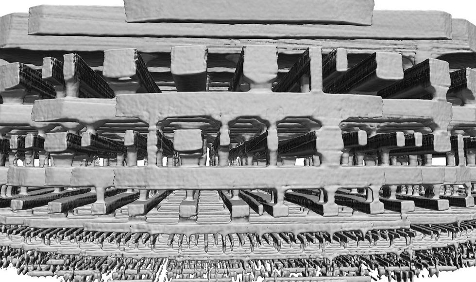 Our first technique, ptychographic X-ray computed tomography, was tested first on a portion of a 22-nanometer Intel processor constructing a detailed 3D image of the chip’s interconnects.SLS-USC Chip-Scan team
Several years later, we’ve made it possible to map the entire interconnect structure of even the most advanced and complex processors without destroying them. Right now, that process takes more than a day, but improvements over the next few years should enable the mapping of entire chips within hours.
This technique—called ptychographic X-ray laminography—requires access to some of the world’s most powerful X-ray light sources. But most of these facilities are, conveniently, located close to where much of the advanced chip design happens. So as access to this technique expands, no flaw, failure, or fiendish trick will be able to hide.
After deciding to pursue this approach, our first order of business was to establish what state-of-the-art X-ray techniques could do. That was done at the Paul Scherrer Institute (PSI) in Switzerland, where one of us (Aeppli) works. PSI is home to the Swiss Light Source (SLS) synchrotron, one of the 15 brightest sources of coherent X-rays built so far.
Coherent X-rays differ from what’s used in a medical or dental office in the same way that the highly collimated beam of light from a laser pointer differs from light emitted in all directions from an incandescent bulb. The SLS and similar facilities generate highly coherent beams of X-ray photons by first accelerating electrons almost to the speed of light. Then, magnetic fields deflect those electrons, inducing the production of the desired X-rays.
To see what we could do with the SLS, our multidisciplinary team bought an Intel Pentium G3260 processor from a local store for about US $50 and removed the packaging to expose the silicon. (This CPU was manufactured using 22-nanometer CMOS FinFET technology).
A fly-though of the top layers of an Intel 22-nanometer processor reconstructed from X-ray scans.SLS-USC Chip-Scan Team
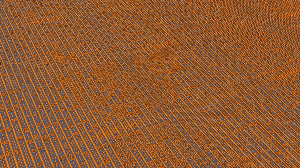
Like all such chips, the G3260’s transistors are made of silicon, but it’s the arrangement of metal interconnects that link them up to form circuits. In a modern processor, interconnects are built in more than 15 layers, which from above look like a map of a city’s street grid. The lower layers, closer to the silicon, have incredibly fine features, spaced just nanometers apart in today’s most advanced chips. As you ascend the interconnect layers, the features become sparser and bigger, until you reach the top, where electrical contact pads connect the chip to its package.
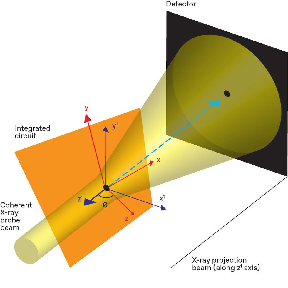
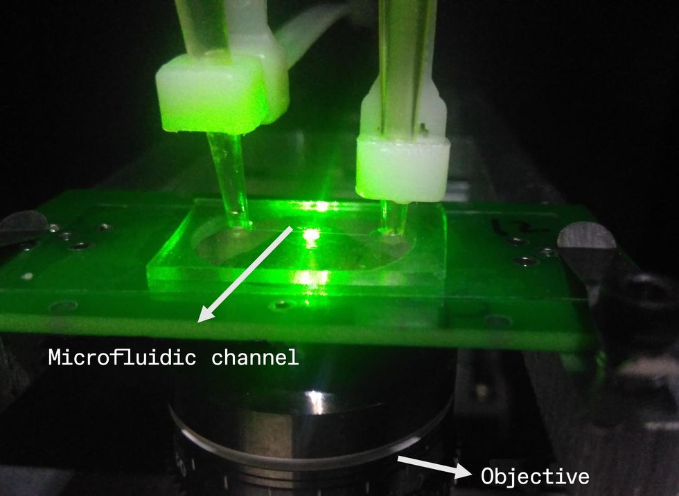
We began our examination by cutting out a 10-micrometer-wide cylinder from the G3260. We had to take this destructive step because it greatly simplified things. Ten micrometers is less than half the penetration depth of the SLS’s photons, so with something this small we’d be able to detect enough photons passing through the pillar to determine what was inside.
We placed the sample on a mechanical stage to rotate it about its cylindrical axis and then fired a coherent beam of X-rays through the side. As the sample rotated, we illuminated it with a pattern of overlapping 2-µm-wide spots.
At each illuminated spot, the coherent X-rays diffracted as they passed through the chip’s tortuous tower of copper interconnects, projecting a pattern onto a detector, which was stored for subsequent processing. The recorded projections contained enough information about the material through which the X-rays traveled to determine the structure in three dimensions. This approach is called ptychographic X-ray computed tomography (PXCT). Ptychography is the computational process of producing an image of something from the interference pattern of light through it.
 SLS-USC Chip-Scan team
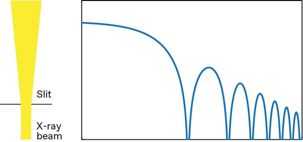
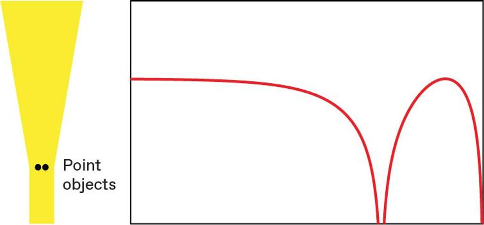
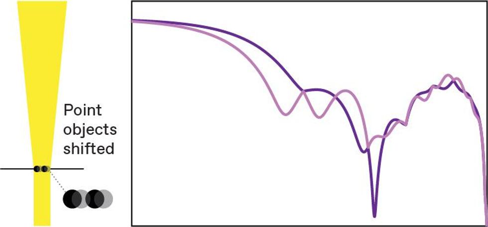
Some fairly simple X-ray diffraction effects reveal enough information to derive nanoscale structures. Shining X-rays through a small slit [top left] projects the classic Fraunhofer pattern onto a detector [blue, top]. Replace the slit with two pointlike objects [center left], spaced closer together than the slit, and a different pattern is projected [red, center]. Placing the point objects within the slit combines the two interference patterns [dark purple, bottom]. Shifting the objects within the slit [bottom left] alters produce a new combination [light purple]. Several such interference patterns together reveal the position of objects in an X-ray beam’s path.
The underlying principle behind PXCT is relatively simple, resembling the diffraction of light through slits. You might recall from your introductory physics class that if you shine a coherent beam of light through a slit onto a distant plane, the experiment produces what’s called a Fraunhofer diffraction pattern. This is a pattern of light and dark bands, or fringes, spaced proportionally to the ratio of the light’s wavelength divided by the width of the slit.
If, instead of shining light through a slit, you shine it on a pair of closely spaced objects, ones so small that they are effectively points, you will get a different pattern. It doesn’t matter where in the beam the objects are. As long as they stay the same distance from each other, you can move them around and you’d get the same pattern.
By themselves, neither of these phenomena will let you reconstruct the tangle of interconnects in a microchip. But if you combine them, you’ll start to see how it could work. Put the pair of objects within the slit. The resulting interference pattern is derived from the diffraction due to a combination of slit and object, revealing information about the width of the slit, the distance between the objects, and the relative position of the objects and the slit. If you move the two points slightly, the interference pattern shifts. And it’s that shift that allows you to calculate exactly where the objects are within the slit.
Any real sample can be treated as a set of pointlike objects, which give rise to complex X-ray scattering patterns. Such patterns can be used to infer how those pointlike objects are arranged in two dimensions. And the principle can be used to map things out in three dimensions by rotating the sample within the beam, a process called tomographic reconstruction.
You need to make sure you’re set up to collect enough data to map the structure at the required resolution. Resolution is determined by the X-ray wavelength, the size of the detector, and a few other parameters. For our initial measurements with the SLS, which used 0.21-nm-wavelength X-rays, the detector had to be placed about 7 meters from the sample to reach our target resolution of 13 nm.
In March 2017, we demonstrated the use of PXCT for nondestructive imaging of integrated circuits by publishing some very pretty 3D images of copper interconnects in the Intel Pentium G3260 processor. Those images reveal the three-dimensional character and complexity of electrical interconnects in this CMOS integrated circuit. But they also captured interesting details such as the imperfections in the metal connections between the layers and the roughness between the copper and the silica dielectric around it.
From this proof-of-principle demonstration alone, it was clear that the technique had potential in failure analysis, design validation, and quality control. So we used PXCT to probe similarly sized cylinders cut from chips built with other companies’ technologies. The details in the resulting 3D reconstructions were like fingerprints that were unique to the ICs and also revealed much about the manufacturing processes used to fabricate the chips.
 SLS-USC Chip-Scan team
In an edge-on position, this chip [orange] is too thick for X-rays to penetrate. But tilting the chip at an angle [see theta, center] makes the cross section thin enough. The mechanical stage the chip sits on [not shown] then rotates the sample within the X-ray beam around the z axis to project interference patterns onto a detector that can be used to reconstruct the chip’s interconnects.
We were encouraged by our early success. But we knew we could do better, by building a new type of X-ray microscope and coming up with more effective ways to improve image reconstruction using chip design and manufacturing information. We called the new technique PyXL, shorthand for ptychographic X-ray laminography.
The first thing to deal with was how to scan a whole 10-millimeter-wide chip when we had an X-ray penetration depth of only around 30 µm. We solved this problem by first tilting the chip at an angle relative to the beam. Next, we rotated the sample about the axis perpendicular to the plane of the chip. At the same time we also moved it sideways, raster fashion. This allowed us to scan all parts of the chip with the beam.
At each moment in this process, the X-rays passing through the chip are scattered by the materials inside the IC, creating a diffraction pattern. As with PXCT, diffraction patterns from overlapping illumination spots contain redundant information about what the X-rays have passed through. Imaging algorithms then infer a structure that is the most consistent with all measured diffraction patterns. From these we can reconstruct the interior of the whole chip in 3D.
Needless to say, there is plenty to worry about when developing a new kind of microscope. It must have a stable mechanical design, including precise motion stages and position measurement. And it must record in detail how the beam illuminates each spot on the chip and the ensuing diffraction patterns. Finding practical solutions to these and other issues required the efforts of a team of 14 engineers and physicists. The geometry of PyXL also required developing new algorithms to interpret the data collected. It was hard work, but by late 2018 we had successfully probed 16-nm ICs, publishing the results in October 2019.
Today’s cutting-edge processors can have interconnects as little as 30 nm apart, and our technique can, at least in principle, produce images of structures smaller than 2 nm.
In these experiments, we were able to use PyXL to peel away each layer of interconnects virtually to reveal the circuits they form. As an early test, we inserted a small flaw into the design file for the interconnect layer closest to the silicon. When we compared this version of the layer with the PyXL reconstruction of the chip, the flaw was immediately obvious.
In principle, a few days of work is all we’d need to use PyXL to obtain meaningful information about the integrity of an IC manufactured in even the most advanced facilities. Today’s cutting-edge processors can have interconnects just tens of nanometers apart, and our technique can, at least in principle, produce images of structures smaller than 2 nm.
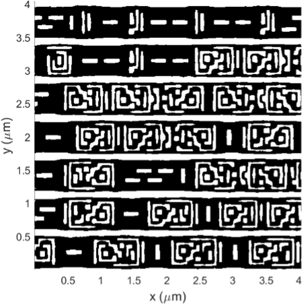
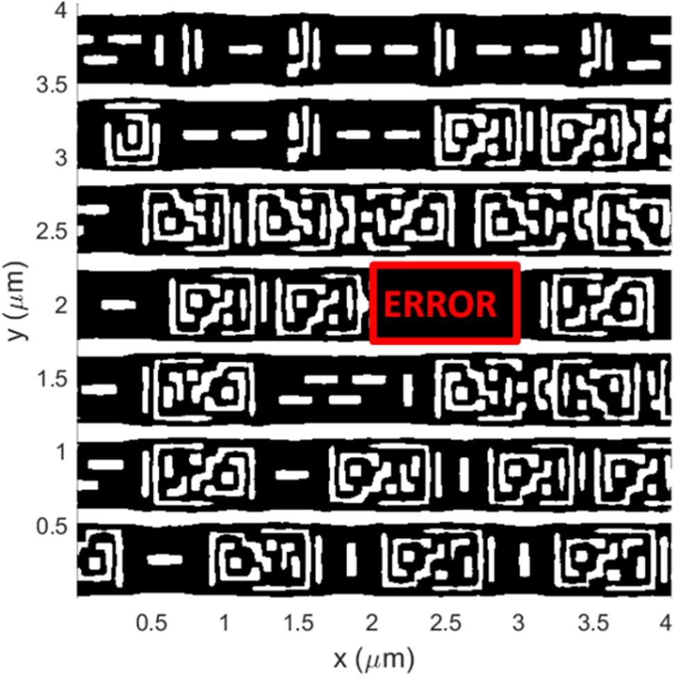
The new version of our X-ray technique, called ptychographic X-ray laminography, can uncover the interconnect structure of entire chips without damaging them, even down to the smallest structures [top]. Using that technique, we could easily discover a (deliberate) discrepancy between the design file and what was manufactured [bottom].
But increased resolution does take longer. Although the hardware we’ve built has the capacity to completely scan an area up to 1.2 by 1.2 centimeters at the highest resolution, doing so would be impractical. Zooming in on an area of interest would be a better use of time. In our initial experiments, a low-resolution (500-nm) scan over a square portion of a chip that was 0.3 mm on a side took 30 hours to acquire. A high-resolution (19-nm) scan of a much smaller portion of the chip, just 40 μm wide, took 60 hours.
The imaging rate is fundamentally limited by the X-ray flux available to us at SLS. But other facilities boast higher X-ray fluxes, and methods are in the works to boost X-ray source “brilliance”—a combination of the number of photons produced, the beam’s area, and how quickly it spreads. For example, the MAX IV Laboratory in Lund, Sweden, pioneered a way to boost its brilliance by two orders of magnitude. A further one or two orders of magnitude can be obtained by means of new X-ray optics. Combining these improvements should one day increase total flux by a factor of 10,000.
With this higher flux, we should be able to achieve a resolution of 2 nm in less time than it now takes to obtain 19-nm resolution. Our system could also survey a one-square-centimeter integrated circuit—about the size of an Apple M1 processor—at 250-nm resolution in fewer than 30 hours.
And there are other ways of boosting imaging speed and resolution, such as better stabilizing the probe beam and improving our algorithms to account for the design rules of ICs and the deformation that can result from too much X-ray exposure.
Although we can already tell a lot about an IC from just the layout of its interconnects, with further improvements we should be able to discover everything about it, including the materials it’s made of. For the 16-nm-technology node, that includes copper, aluminum, tungsten, and compounds called silicides. We might even be able to make local measurements of strain in the silicon lattice, which arises from the multilayer manufacturing processes needed to make cutting-edge devices.
Identifying materials could become particularly important, now that copper-interconnect technology is approaching its limits. In contemporary CMOS circuits, copper interconnects are susceptible to electromigration, where current can kick copper atoms out of alignment and cause voids in the structure. To counter this, the interconnects are sheathed in a barrier material. But these sheaths can be so thick that they leave little room for the copper, making the interconnects too resistive. So alternative materials, such as cobalt and ruthenium, are being explored. Because the interconnects in question are so fine, we’ll need to reach sub-10-nm resolution to distinguish them.
There’s reason to think we’ll get there. Applying PXCT and PyXL to the “connectome” of both hardware and wetware (brains) is one of the key arguments researchers around the world have made to support the construction of new and upgraded X-ray sources. In the meantime, work continues in our laboratories in California and Switzerland to develop better hardware and software. So someday soon, if you’re suspicious of your new CPU or curious about a competitor’s, you could make a fly-through tour through its inner workings to make sure everything is really in its proper place.
The SLS-USC Chip-Scan Team includes Mirko Holler, Michal Odstrcil, Manuel Guizar-Sicairos, Maxime Lebugle, Elisabeth Müller, Simone Finizio, Gemma Tinti, Christian David, Joshua Zusman, Walter Unglaub, Oliver Bunk, Jörg Raabe, A. F. J. Levi, and Gabriel Aeppli.
This article appears in the May 2022 print issue as “The Naked Chip.”
Reference: https://ift.tt/mlHEsoC


Video Friday is your weekly selection of awesome robotics videos, collected by your friends at IEEE Spectrum robotics. We also post a weekly calendar of upcoming robotics events for the next few months. Please send us your events for inclusion.
Enjoy today's videos!
I'm not sure it's geographically appropriate for a Husky robot to be this close to penguins in Antarctica, but on the other hand, who cares, because I am all in for robots and penguins.
The project consists of a hybrid (autonomous and remote-controlled) Husky UGV-based robot named ECHO that carries a variety of sensors including a camera and an RFID antenna to read RFID tags from chipped penguins (the kind of chips that are also used to chip dogs and cats). With the RFID scanner, ECHO will scan penguins to assess their breeding status and survival success. Overall, the robot will be able to track individual penguins throughout their lifetimes, allowing researchers to gather data for behavioral and population dynamics research.
[ Clearpath ]
Snap has launched a little camera drone called Pixy. It's nothing special, but that's fine: it looks to be small, safe, and quite easy to use. And I really appreciate that this video seems to show actual footage from the drone, which is not fantastic, but totally workable.
$250 seems a bit steep, but perhaps the safe form factor and ease of use could make it worthwhile.
[ Pixy ]
This is pretty awesome- it's a RoboCup standard platform event where the robots are operating fully autonomously. Watch right after kick-off as the robot in the black jersey (closest to the ball) books it off screen to the left. As it turns out, she (her name is Sarah) went deep into the opponent's half, where she camped out by the goal, in a perfect position to recieve a brillant pass.
[ B-Human ]
GITAI has already demonstrated its robotic arm inside of the International Space Station, and now it look like they're getting ready to work outside of the station as well.
[ GITAI ]
Things that I want robots to do so that I don't have to: Waste sorting.
Weird to have them call the robot both "she" and "unmanned" in practically the same sentence.
[ ZenRobotics ]
At Agility, we make robots that are made for work. Our expertise is marrying design, software, and hardware to build robots that are capable of doing limitless tasks as part of a blended human-robot workforce.
OK, I really want to know if Digit can use that step stool at the back of the trailer.
[ Agility ]
Zimbabwe Flying Labs' Tawanda Chihambakwe shares how Zimbabwe Flying Labs started using drones for STEM programs and how drones impact conservation and agriculture.
[ ZFL ]
Robotics has the potential to revolutionize our daily lives, enabling humans to do things never thought possible. SRI is at the forefront of developments that have and will continue to redefine manufacturing, medicine, safety, and so much more.
[ SRI ]
A drone show from CollMot, who seems to use much larger drones than anyone else.
[ CollMot ]
Reference: https://ift.tt/QrOz4hn

Imagine sensors that can detect the magnetic fields of thoughts, help lunar rovers detect oxygen in moon rocks, or listen to radio waves from dark matter. Just as quantum computers can theoretically find the answers to problems no classical computer could ever solve, so too can an emerging generation of quantum sensors lead to new levels of sensitivity, new kinds of applications, and new opportunities to advance a range of fields, technologies, and scientific pursuits.
Quantum technology relies on quantum effects that can arise because the universe can become a fuzzy place at its very smallest levels. For example, the quantum effect known as superposition allows atoms and other building blocks of the cosmos to essentially exist in two or more places at the same time, while another quantum effect known as entanglement can link particles so they can influence each other instantly regardless of how far apart they are.
These quantum effects are infamously fragile to outside interference. However, whereas quantum computers strive to overcome this weakness, quantum sensors capitalize on this vulnerability to achieve extraordinary sensitivity to the slightest disturbances to the environment. Below are just a small sampling of the many kinds and varieties of quantum sensors being developed and deployed today.
BRAIN SCANS: Electric currents within the brain generate magnetic fields that sensors can analyze to non-invasively scan brain activity. Now quantum sensors are enabling a wearable helmet to perform such magnetoencephalography (MEG) scans with unprecedented performance and cost.
Currently MEG scans are performed with sensors known as superconducting quantum interference devices (SQUIDs). These require cooling with expensive liquid helium to minus 269 degrees Celsius, making the scanners extremely large. In contrast, the new devices from startup Cerca Magnetics in Nottingham, England, are each about the size of a Lego brick.
Each device, called an optically pumped magnetometer (OPM), contains a laser that shines a beam through a cloud of rubidium atoms at a light detector. The beam can make the magnetic fields of the rubidium atoms all line up, rendering the cloud essentially transparent. Tiny magnetic fields, such as those from brain activity, can disturb these atoms, making them capable of absorbing light, which the light detector can sense, and the laser resets the cloud so it can continue responding to magnetic disturbances.
The fact these quantum sensors work at room temperature make them much less bulky than SQUIDs. This means they can get placed much closer to a person's head, resulting in a signal at least two times better and theoretically up to five times better, for magnetic images with millimeter accuracy and millisecond resolution of surface areas of the brain, says Matthew Brookes, chairman of Cerca and a researcher at the University of Nottingham.
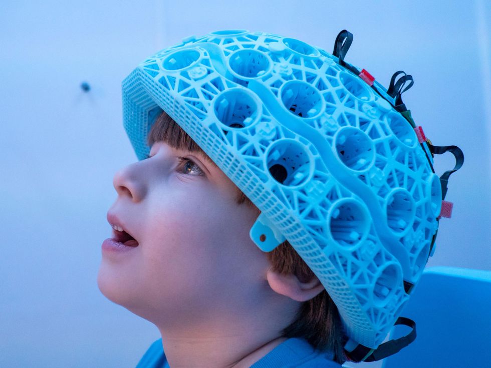 Cerca Magnetics wearable MEG helmets can, the company says, safely be worn by even an active child.Cerca Magnetics
The small, lightweight nature of the sensors also means they can get mounted in a wearable helmet to let people move freely during scanning, instead of having them remain still for very long times as is currently the case. In addition, it can adapt to different head shapes and sizes, making it possible to scan not just adults, but also children and babies. Moreover, "MEG with OPMs is in principle quite a lot cheaper than with SQUIDs," Brookes says. "Even now, in early days with OPMs, a full MEG imaging system is still half the price of a SQUID system for similar performance."
The Cerca scanner can help probe neurological disorders such as epilepsy, concussions, dementia and schizophrenia, "helping shed light on many severe and debilitating conditions," he says.
Future research can aim to push these sensors closer to their theoretical limits of sensitivity, permit more freedom of movement to perhaps let people walk, and add virtual reality and machine learning to boost what researchers can do with the scanners on the experimental and analytical fronts, Brookes says.
GRAVITY MAPPING: A new quantum sensor that maps the strength of Earth's gravitational field can help reveal features hidden underground.
Anything that has mass possesses a gravitational field. The strength of this field's pull depends on a body's mass. Since Earth's mass is not spread out evenly, this means the planet's gravity is stronger at some places than others.
For decades, gravity mapping has uncovered details on large-scale geological activity, but employing such gravity cartography on the scale of meters is challenging, since long measuring times are needed to account for local noise, such as vibrations from nearby traffic.
The new quantum sensor uses clouds of rubidium atoms cooled to a few millionths of a degree Celsius above absolute zero. Laser pulses drive the atoms into states of superposition, with two versions of the atoms falling down slightly different trajectories, and these atoms are then recombined. Then, due to the wave-particle duality—the quantum phenomenon where particles can act like waves, and vice versa—these atoms quantum mechanically interfere with each other, with their peaks and troughs augmenting or suppressing each other. Analyzing the nature of this interference, a technique known as atom interferometry, can reveal the extent of the slightly different gravitational pulls felt along their separate paths.
The sensor uses an hourglass design, with one cloud in each half of the device separated vertically by 1 meter. As such, the sensor can analyze the strength of Earth's gravity at two different heights at the same location. By comparing the data from these clouds, the researchers can account for a variety of sources of noise. In experiments, the sensor could detect a 2-by-2-meter utility tunnel buried roughly 0.5 meters under a road surface between two multistory buildings in the city of Birmingham, England.
Potential applications for the sensor include seeing hidden underground structures, detecting subterranean natural resources, discovering underground archaeological sites, and monitoring volcanic activity and groundwater flows.
The initial refrigerator-size sensor was about 300 kilograms and used about 750 watts. The scientists are now working to build a backpack-size sensor about 20 kilograms that runs on batteries, says Michael Holynski, an experimental physicist at the University of Birmingham in England and director of the startup Delta-G, which is commercializing the sensor. "The current target is to reach a commercial prototype of a next-generation sensor over the next two years," he says. "The early markets are at around the £100 million mark for the sensors themselves. However, the data they will create is more valuable, and relevant to applications that are a few percent of GDP in the U.K."
DETECTING COVID: Another promising quantum sensor could lead to faster, cheaper and more accurate tests for the SARS-CoV-2 virus behind the global pandemic. It relies on microscopic artificial diamonds with defects within them, in which a carbon atom is replaced with a nitrogen atom and the adjacent carbon atom is missing. This defect in the crystals behaves like a tiny magnet whose alignment is very sensitive to magnetic fields, helping such "nitrogen-vacancy centers" serve as sensors.
The new technique involves coating nitrogen-vacancy center diamonds roughly 25 nanometers wide with magnetic compounds that detach from the gems after they bond with the specific RNA sequence of the SARS-CoV-2 virus. When these diamonds are lit with green light, they will emit a red glow. The magnetic coating dims this glow; exposing the sensors to the virus can increase this glow.
The current gold-standard test for the SARS-CoV-2 takes several hours to create enough copies of the virus' genetic material to detect. Moreover, it cannot quantify the amount of virus present with high accuracy and might have false negative rates of more than 25 percent. In contrast, computer simulations suggest the new test can theoretically work in just a second, is sensitive enough to detect just a few hundred strands of the viral RNA, and could have false negative rates below 1 percent.
 The above quantum sensor for the presence of the SARS-CoV-2 virus uses only low-cost materials. The devices could be scaled up, according to the researchers, to analyze a full batch of samples at once.MIT
The nano-diamonds and the other materials used in the test are cheap. In addition, this new method could be adapted to virtually any virus, including any new ones that may emerge, by adjusting the magnetic coating to match the target virus. They are currently synthesizing and testing the sensors to see how well they actually perform. "We hope to get promising results very soon," says researcher Changhao Li, a quantum engineer at MIT.
PROBING CELLS AND MOLECULES: Quantum diamond sensors can also find use in thermometers inside cells. Nitrogen-vacancy centers in diamonds are very sensitive to small temperature fluctuations. Physicist Peter Maurer at the University of Chicago and his colleagues have injected nanometer-scale diamonds with such defects into living cells and examined how the crystals responded to laser beams in order to map temperatures within the cells to a few thousandths of a degree Celsius.
"You can imagine using such atomic-scale thermometers to investigate how temperature influences cell division, gene expression, and how molecules go in and out of cells, all major questions in medicine and biology," says experimental physicist David Awschalom at Argonne National Laboratory and director of the Q-NEXT consortium.
In addition, Maurer and his colleagues are investigating using diamonds with nitrogen-vacancy centers to essentially perform MRI scans on molecules. "With quantum sensors, you can perform MRI to the level of single molecules to understand the relationship between their structure and function, which could radically improve our understanding of medicine," Awschalom says.
The scientists developed a new way to tether single protein and DNA molecules onto the surface of diamonds that host nitrogen-vacancy centers. By analyzing the magnetic fields of these molecules, "you can understand the distances between atoms, the strengths of the interactions between them, where they are and what keeps them together," Awschalom says.
QUANTUM ACCELEROMETER: The world now relies heavily on global navigation satellite systems such as GPS, but the satellite links that help enable such positioning, navigation and timing do not work underground or underwater and are vulnerable to jamming, spoofing and weather. Now a quantum sensor from Imperial College London and Glasgow-based company M Squared can help ships navigate even when GPS is denied.
The quantum sensor is an atom interferometer like the gravity-mapping device. Analyzing how the phase of its atomic wave-packets shifts can reveal any acceleration or rotation they experienced, which the device can use to calculate the change in its position with time.
This quantum accelerometer can help serve as the foundation of an inertial navigation system that does not rely on any outside signals. Whereas temperature fluctuations and other factors lead the position estimates of conventional inertial navigation systems to drift within hours without an outside reference signal, M Squared's device experience negligible drift even after days, says Joseph Cotter, a research fellow at Imperial College London's Center for Cold Matter.
"The early adopters of this emerging quantum technology are likely to be those interested in long-range navigation for underwater and surface vehicles," Cotter says. "However, as the technology develops and becomes increasingly compact and lower cost, it will have wider benefits across the transportation industry through deployment on ships, trains, and aircraft."
The researchers have field tests planned for their latest device this summer. Currently the quantum accelerometer "is about the size of two washing machines," Cotter notes. "We're working to get it even more compact."
QUANTUM SOFTWARE: Where most quantum sensor companies focus on the hardware, Sydney-based startup Q-CTRL focuses on software to enhance quantum technology. "When you take quantum sensors out of pristine lab environments out into the field, you often see a huge degrading in performance due to noise in the platforms," says Michael Biercuk, CEO and founder of Q-CTRL. "Our focus is recapturing this performance with our quantum control software."
For instance, many quantum sensors use lasers to scan cold atoms to detect any changes in the environment, but any movement in the device can lead the atoms to move out of the laser beams. "With our software, we can shape the pulse of light—its frequency, amplitude, phase—to make it more resilient against motion without any changes to the hardware itself," Biercuk says.
Q-CTRL is partnering with Sydney-based inertial navigation company Advanced Navigation to develop a rubidium-based atom-interferometer inertial navigation system that can fit in less than one cubic meter and can work in GPS-denied areas. "We aim to have the first delivery of fieldable systems in 2023," Biercuk says.
The company also aims to place atom interferometers onboard satellites to perform gravity mapping from space at 100 times less than the current cost, with launches of demonstration payloads into low Earth orbit expected in 2025. In addition, Q-CTRL is a member of Australia's Seven Sisters space industry consortium designing a new lunar rover in support of NASA's Artemis program, in which Q-CTRL is working on a rubidium-based quantum atomic magnetometer to magnetically analyze lunar rocks for oxygen.
DARK MATTER, GIANT TELESCOPES: Quantum sensors may help probe matters far beyond Earth. For example, one of the greatest mysteries in the universe is the nature and identity of dark matter, the invisible substance thought to make up five-sixths of all matter in the universe. Leading theoretical candidates for dark matter include particles known as axions, which in principles have an exceedingly low mass, at most just a trillionth the mass of the proton, making them difficult to detect.
Quantum physicist Kent Irwin at Stanford University and his colleagues are developing a "dark matter radio" to detect axions and similar dark matter candidates. A powerful magnet in the device will convert axions into radio waves, and quantum sensors will aim to amplify and detect these extremely weak radio signals.
Since the frequencies the dark matter radio will probe will include ones used for over-the-air broadcasting, the device will require shielding within a thin layer of superconducting niobium metal cooled in liquid helium. This should screen out artificial signals but will be easily penetrated by dark matter. "We're planning a version of the dark matter radio now that's about a cubic meter in scale that we'd like to build in the next few years," Irwin says.
Quantum physics may also help enable giant telescope arrays, Irwin says. Multiple telescopes widely separated in space can theoretically be combined to essentially form a single telescope thousands of kilometers wide.
Forming such arrays with optical telescopes imaging visible light is difficult because of random fluctuations that inevitably crop up in any fiber optics linking these telescopes. However, entanglement can in principle allow quantum teleportation of data across great distances.
Quantum optics researcher Paul Kwiat at the University of Illinois at Urbana–Champaign is currently investigating such "quantum-enhanced telescopy" with tabletop experiments. "It's still very far off, but also a true holy grail, a moonshot that's incredibly exciting," Irwin says. A telescope array roughly the diameter of Earth may in principle image features the size of cities on nearby stars, he says.
UNTOLD LIMITS: Recently scientists in Austria developed the first programmable quantum sensor, a device capable of an unprecedented level of sensitivity operating near the fundamental limits imposed by the laws of quantum mechanics.
In this work, they programmed a quantum computer to find the best settings for itself with which to measure the states of its components. They found this programmable quantum sensor could optimize itself enough to approach the fundamental sensing limit up to a factor of about 1.45. (The closer a sensor approaches the ultimate sensing limit of 1, the better its performance.) They suggest programmable quantum sensors could find use in devices such as atomic clocks and global positioning systems, as well as magnetic and inertial sensors.
All in all, "quantum sensors are emerging with exquisite precision to cover everything from single proteins all the way to questions in astronomy and cosmology," Awschalom says.
Reference: https://ift.tt/TsYSart

This sponsored article is brought to you by Robotics Summit & Expo.
The Robotics Summit & Expo is returning to Boston on May 10-11 at the Boston Convention and Exhibition Center!
This international event will bring attendees content that will help them to design, development, manufacture, and deliver commercial-class robots.

Register now and save 25% on your full conference pass by using code RSE25 at checkout.
This year's program has an exceptional lineup of speakers covering trending topics in the industry such as interoperability, cloud technology, autonomous mobile robots, human scale automation, collaborative robots, motion control and so much more within the five dedicated tracks of the program.
Attendees will hear keynote presentations from industry thought leaders including:
Not only does our event provide our attendees with educational sessions and access to some of the leading robotics companies around the nation but we also have complimentary events and unlimited networking opportunities for our attendees, including a reception on the expo floor, a career fair after the event, and a chance to walk Boston Dynamic's Spot quadruped.
Attendees will have access to two additional co-located events: The Healthcare Robotics Engineering Forum and DeviceTalks Boston.
For an additional bonus, you can save 25% on your full conference pass right now by using code RSE25 at checkout!
Reference: https://ift.tt/fNpda7q


The World Health Organization (WHO) declared the outbreak of the COVID-19 pandemic on 11 March 2020. Two years later, it put the cumulative number of cases at about 452 million, more than 5 percent of the world’s population, and the number of new infections was still averaging more than a million a day.
How many people have died? We can begin to model the problem by using the highest mortality estimates of the two previous major pandemics—138 deaths per 100,000 people in 1957–1958 and 111 per 100,000 in 1968–1969. A similarly virulent two-year event, adjusted for today’s population of 7.9 billion, would then be expected to kill 8.8–10 million people. On 11 March 2022, the WHO’s officially logged COVID death toll was about 6 million. Every epidemiologist knows that this must be a significant underestimate.
A better way to assess the death toll is to calculate excess mortality, that is, the difference between the total number of deaths during a crisis and the deaths that would be expected under normal conditions. Obviously, this approach will work only in those countries that collect near-impeccable mortality statistics. The WHO has assessed the health-information capacity of 133 countries, showing that the share of all deaths that are registered ranges from 100 percent in Japan and 98 percent in the European Union to 80 percent in China and only 10 percent in Africa. Given these realities, calculations of excess mortalities are revealing in France, inaccurate in China, and impossible in Nigeria.
And even in Japan, interpreting excess mortalities can be complicated. On one hand, COVID excess mortality includes not only the deaths directly attributable to the virus (due to inflammation of tissues or oxygen deprivation) but also the indirect effects caused when COVID aggravates preexisting conditions (heart disease, dementia) or induces the deterioration and disruption of normal health care (forgone diagnoses and treatments). But on the other hand, the spread of COVID appears to have largely preempted seasonal excess mortality caused by winter flu epidemics among the elderly, and lockdowns and economic slowdowns improved the quality of outdoor air.
The officially logged COVID death toll is about 6 million; every epidemiologist knows that this must be a significant underestimate.
By the end of 2020 the official worldwide COVID death toll was 1.91 million, but the WHO’s preliminary evaluation estimated at least 3 million deaths. According to Seattle’s Institute for Health Metrics and Evaluation (IHME), which counts only cases caused directly by the virus, not by the pandemic’s disruption of health care, excess global mortality reached 15.34 million (that is, between 12.6 and 18.9 million) by 11 March 2022. That’s the second anniversary of the beginning of the pandemic, according to the WHO’s reckoning.
A model run by The Economist relies on scores of national indicators correlating with data on excess death and thus it has produced a wide range of estimates. For the pandemic’s 2-year mark, the range is between 14 million (2 times the official tally of 6.86 million) and 23.7 million (3.5 times the official number), with the central value at 20 million (2.9 times the official total). And on 10 March 2022, The Lancet, one of the world’s leading medical journals, published its excess mortality estimate for 2020 and 2021: 18.2 (17.1 to 19.6) million, nearly 3.1 times the official two-year tally.
Even using a toll of around 15 million deaths is enough to put COVID-19 far ahead of the two major post-1945 pandemics on a per capita basis. And any number above 20 million would make it in absolute terms (but not in relation to population) an event on the same order of magnitude as the great 1918–1920 influenza pandemic. Will we ever know the real toll to within 10 percent, plus or minus?
Reference: https://ift.tt/kSNqxQY


Enlarge (credit: Getty Images)
Vulnerabilities recently discovered by Microsoft make it easy for people with a toehold on many Linux desktop systems to quickly gain root system rights— the latest elevation of privileges flaw to come to light in the open source OS.
As operating systems have been hardened to withstand compromises in recent years, elevation of privilege (EoP) vulnerabilities have become a crucial ingredient for most successful hacks. They can be exploited in concert with other vulnerabilities that on their own are often considered less severe, with the latter giving what’s called local access and the former escalating the root access. From there, adversaries with physical access or limited system rights can deploy backdoors or execute code of their choice.
Nimbuspwn, as Microsoft has named the EoP threat, is two vulnerabilities that reside in the networkd-dispatcher, a component in many Linux distributions that dispatch network status changes and can run various scripts to respond to a new status. When a machine boots, networkd-dispatcher runs as root.


Enlarge / The first Meta Store won't necessarily be your one-stop shop for all things sold by Meta—as this artistic interpretation points to one thing not sold by the store until further notice. (credit: Aurich Lawson | Getty Images)
On May 9, Meta will double down on its metaverse sales pitch by... making people drive to California to sample its wares at a single physical location.
The uncreatively named Meta Store will showcase every physical product the company sells under its various branded umbrellas, particularly the Meta Quest 2 VR system (formerly Oculus Quest 2). The company's first retail store will be housed in a 1,550-square-foot space on Meta's Burlingame, California, campus, which houses a number of Meta's VR- and AR-specific development efforts, and it will allow the public to test and purchase any of Meta's physical products.

A photo of the first Meta Store, as provided by Meta. (credit: Meta)
But it's not a comprehensive Meta sales location, as its shelves will not include access to the reams of user data accumulated by the company's network of criss-crossed sites—though we'll keep our eyes peeled in case the Meta Store decides to unveil a Cambridge Analytica-themed aisle in the future.


Enlarge (credit: Getty Images)
Malicious hackers have been hammering servers with attacks that exploit the recently discovered SpringShell vulnerability in an attempt to install cryptomining malware, researchers said.
SpringShell came to light late last month when a researcher demonstrated how it could be used to remotely execute malicious code on servers that run the Spring model-view-controller or WebFlux applications on top of Java Development Kit versions 9 or higher. Spring is the most widely used Java framework for developing enterprise-level applications in Java. The framework is part of a sprawling ecosystem that provides tools for things like cloud, data, and security apps.
Earlier this month, security firm Trend Micro said it began detecting attempts. From April 1 to April 12, company researchers detected an average of roughly 700 attempts per day to exploit the vulnerability to install cryptomining software. By running the malware on powerful enterprise servers, criminals can mine Bitcoin or other types of digital cash using the resources and electricity of an unwitting victim.
A version of this post originally appeared on Tedium , Ernie Smith’s newsletter, which hunts for the end of the long tail. Personal c...


