
Monday, March 25, 2024

Inkjets Are for More Than Just Printing


In the early 1980s, offices were noisy places, filled with the sound of metal striking inked ribbons to mark characters on paper. IBM Selectric typewriters clacked, daisy wheel printers clattered, and dot-matrix printers made loud ripping sounds.

Today, those noises are gone. And though we do spend more time reading on screens, we haven’t stopped printing on paper.

The main reason for the quiet? The inkjet printer. While laser printers do the big printing jobs in commercial settings, the inkjet printer has become the printer most of us use at home and at the office.

The printhead of an inkjet printer performs a remarkable task. Even at the coarse resolution of 96 dots per inch (dpi), as was typical for the first models in the 1980s, the distance from dot center to dot center is a mere 260 micrometers. To fill a standard letter page that has 2.5-centimeter margins would require more than half a million individual ink droplets. Delivery of those tiny droplets involves moving them with very precise control, repeated a vast number of times as rapidly as possible. This process is ideally suited for microelectromechanical systems (MEMS), which are electronic devices with microscopic components that employ movement.

If there is a way to package something in microscopic droplets with the appropriate fluid properties, chances are someone is looking to adapt inkjet technology to work with it.

As with all microtechnology, the specs of inkjet systems have evolved considerably over time. A typical inkjet printhead in the mid-1980s had 12 nozzles working in parallel, each one emitting up to 1,350 droplets per second, to print 150 alphanumeric characters per second. Today, a high-end inkjet printhead used in a commercial printing press may contain 21,000 nozzles, each nozzle printing 20,000 to 150,000 dots per second. Each drop of ink may be just 1.5 picoliters—a picoliter is one-trillionth of a liter—and measure roughly 14 micrometers in diameter.

Surpassing the visions of its creators, the inkjet technology used in these printers has found a host of applications beyond putting dots on paper. These include making DNA microarrays for genomics, creating electrical traces for printed circuit boards, and building 3D-printed structures. Future uses could include personalized medicine and development of advanced batteries.

Indeed, a search for patents containing the word “inkjet” today returns more than 92,000 results. If there is a way to package something in microscopic droplets with the appropriate fluid properties, chances are someone is looking to adapt inkjet technology to work with it.

How MEMS Transformed Inkjet Printing

Inkjet technology dates back to 1948, when Swedish inventor Rune Elmqvist patented a chart recorder wherein a very thin glass tube emitting a continuous jet of ink was steered to make a trace on a moving strip of paper. A couple of years later, he demonstrated his invention in the form of a device for recording electrocardiograms.

In 1965, Richard G. Sweet of Stanford University developed a chart recorder in which the jet of ink was broken into a uniform stream of electrically charged droplets. Diverter electrodes on either side of the stream could permit the drops to proceed straight to the paper, or else deflect them onto an absorbent pad or into a gutter to be collected and reused.
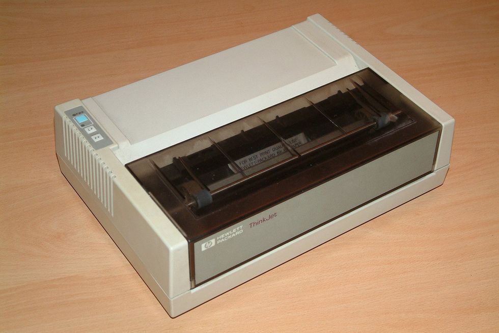
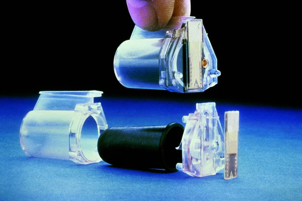
Photos of HP Thinkjet printer, ink cartridge, and HP Jet Fusion 5200 3D printer. In April 1984, the HP ThinkJet [top] ushered in the era of desktop inkjet printing. The Thinkjet’s ink cartridge [bottom] delivered thousands of microscopic droplets a second from 12 nozzles. The MEMS technology to perform that feat was entirely within the printhead.HP

This technology is called continuous inkjet printing, and by 1976 IBM had incorporated it in a commercial printer, the IBM 6640. But continuous inkjets lose ink to evaporation even when recycling is used, limiting their appeal.

To get around the wastefulness of continuous inkjets, others worked on developing drop-on-demand inkjet printers, where each orifice on the printhead emits one drop of ink at a time, avoiding the waste of a continual flow of drops. Surface tension holds the ink in place in a tiny open nozzle until a mechanism pushes the ink to eject a drop. Each drop hitting the paper creates a dot, and moving the printhead back and forth builds up an image. A printhead with multiple orifices can emit many drops of ink simultaneously, so each pass of the printhead across the page adds a strip of the image, not just a single drop-thin line.

In the late 1970s, Siemens was the first to sell a drop-on-demand inkjet printer. It came not as a stand-alone device like a modern desktop printer, but as an integral part of a computer terminal, the Siemens PT80i (Printer Terminal 80 Inkjet). The printer used piezoelectric actuators surrounding 12 ink tubes, which fed 12 nozzles to shoot ink droplets, printing 270 characters per second.

Piezoelectric devices rely on how some materials, such as ceramic lead-zirconate-titanate (PZT), change shape when subjected to a voltage. This effect has proved extremely useful in MEMS in general, for generating precise forces and motion on command. If a layer of PZT is bonded to a nonpiezoelectric material, forming what’s called a bimorph, it will bend when exposed to a voltage. In the piezoelectric inkjet nozzle, the bending of the bimorph pushes ink out of the orifice. [For another application of piezoelectric MEMS technology, see “How Ultrasound Became Ultra Small.”]
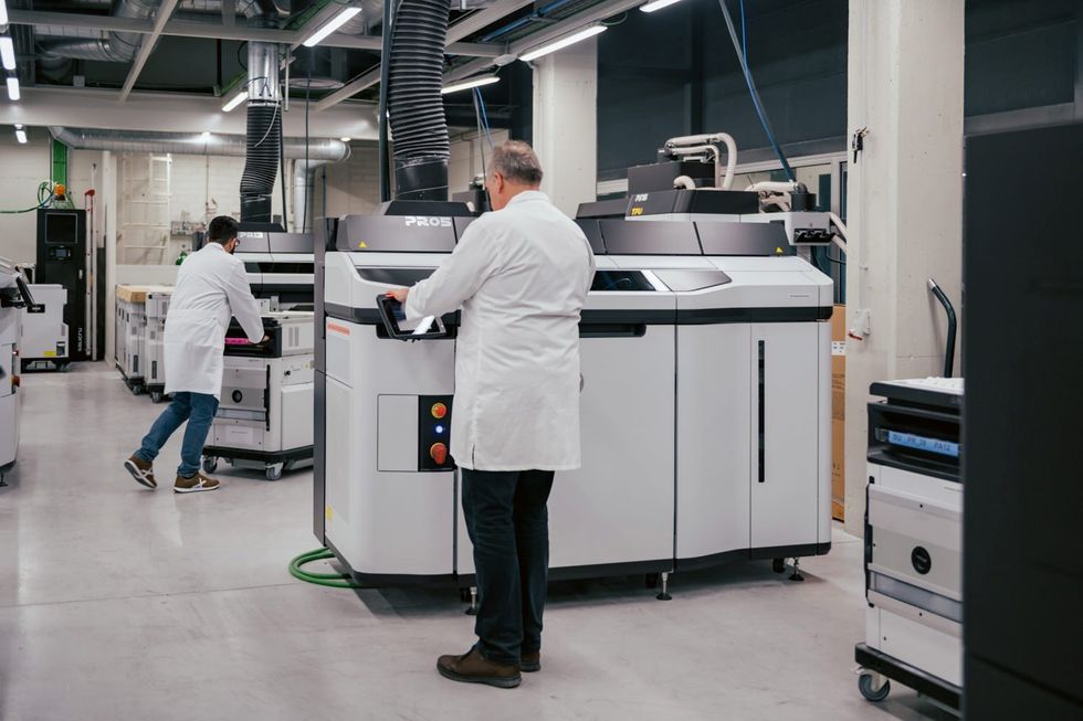
Photo of HP Jet Fusion 5200 3D printer The HP Jet Fusion 5200 industrial 3D printer uses an inkjet process to build parts out of nylon, polypropylene, or polyurethane.HP

This novel printing technology, however, was not yet as dependable as proven impact printers in the 1970s, and the whole Siemens terminal became unusable if the printer failed, so it didn’t catch on.

Meanwhile, researchers at both Hewlett-Packard and Canon noticed that ink would boil and splatter when exposed to a hot element like a soldering iron, and they decided to turn that splattering into a useful inkjet printing mechanism. They knew that a resistor could be used as a heating element and could be miniaturized with the same technology as that used for integrated circuits. In the printers they built, each ink nozzle contains a resistor instead of a piezoelectric actuator. An electrical pulse heats the resistor, which flash-boils a thin layer of the ink, forming a rapidly expanding vapor bubble that pushes a droplet of ink out through the orifice.

This work led to two competing versions of thermal inkjet technology coming to market at nearly the same time 40 years ago. (The same year, 1984, Epson introduced a stand-alone piezoelectric inkjet printer.)

Hewlett-Packard’s HP ThinkJet was its first desktop inkjet printer based on its thermal technology, and it was designed to connect to a personal computer for everyday printing. It had an immediate advantage over the recently developed laser printers: It was much cheaper. A desktop laser printer from HP cost US $3,500 (about $10,500 today); HP’s 2225A ThinkJet cost only $495 ($1,500 today). Inkjet printers also used far less power than laser printers did and were quieter. Admittedly, inkjets didn’t have great resolution—96 dpi compared with 300 for laser printers in those early days—and they were slow.

But the advantages outweighed the disadvantages (more so as the technology improved), and inkjet printers came to dominate the desktop and home printer markets. Today, more than 20 companies make inkjet printers, generating a market of more than $100 billion annually and continuing to grow at more than 8 percent per year.

Printing DNA Microarrays With Inkjets

While the business of making inkjet printers matured and grew, some companies began exploring what other kinds of “ink” might be delivered with an inkjet. One of these was Agilent Technologies, a spin-off of Hewlett Packard with a focus on life-science and chemical-analysis technologies. Agilent developed a way to print strands of DNA from the four nucleic acid bases—cytosine (C), guanine (G), adenine (A), and thymine (T). Specifically, the company adapted existing DNA chemistries plus inkjet printing techniques to build microarrays of DNA on glass slides for genomics work, such as measuring which genes are being expressed in an organism under various conditions. Academic researchers have shared open-source methods for converting existing inkjet printers to build their own microarrays, albeit with specs that are much more modest than the commercial systems.

A DNA microarray consists of a substrate, usually glass, with an array of small regions called spots where DNA strands are attached. Agilent produces arrays with as many as a million spots on a single 2.5-by-7.6-cm slide. An open-source system puts up to 10,000 in a somewhat smaller area. Each DNA strand is made of sequences of the bases C, G, A, and T. In double-stranded DNA, the strands have complementary sequences, which join up like rungs of a ladder, C joining with G, and A with T.
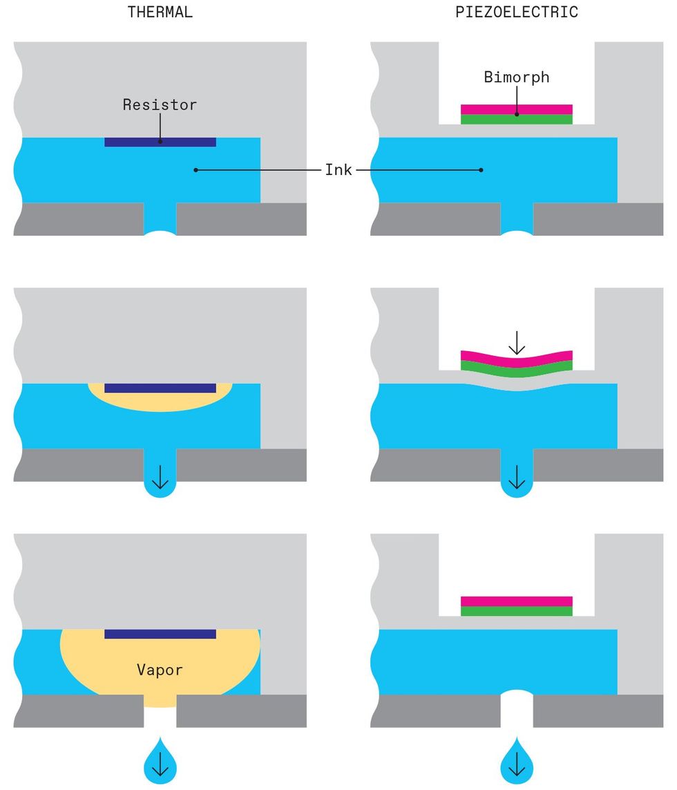

An illustration of the two different types of inkjet nozzles.

In the resting state [top] of an inkjet nozzle, the ink is held in place by surface tension. In a thermal inkjet nozzle [left], a voltage pulse to the heating resistor flash-vaporizes a thin layer of ink, producing an expanding vapor bubble [left, middle] that pushes a droplet of ink out through the orifice [left, bottom]. In less than a millisecond the vapor recondenses and the chamber cools and refills with ink, returning the nozzle to the resting state. A piezoelectric inkjet nozzle [right] is driven by a piezoelectric bimorph, which bends when a voltage is applied [right, middle] to push out an ink droplet [right, bottom].

A DNA microarray uses single-stranded DNA, and each spot has millions of strands with a common sequence. When a sample with copies of the complementary strand washes over the spot, those strands bind together with the strands anchored in the spot. The sample strands are tagged with fluorescent molecules, and the user learns which DNA sequences were present in the sample by examining which spots light up.

In Agilent’s method for fabricating a microarray, the printer makes multiple passes over the substrate, each pass adding one base to each strand in the spots, with intermediate steps to prepare for the next pass.

Adding a base is actually a three-step process. Each of the growing strands in the microarray spots has a molecular “cap” at the end that prevents the indiscriminate addition of more bases. So the first step is to remove or deactivate those caps by washing a solution over the nascent microarray. The second step is analogous to printing a page: At each spot on the microarray, the inkjet adds a dot of liquid containing the next monomer molecule (modified versions of C, G, A, or T) to be added to the end of the strand. These monomers each include a new cap so that only one molecule gets added to each strand. Although the newly added monomers are now attached to the strands, the connection is not fully stable, and so the third step applies an oxidizer solution that modifies the bonds, fully integrating the new monomers into the DNA structure. Rinse and repeat.

The versatility of the open-source inkjet construction allows researchers to rapidly build prototype arrays with whatever sequences they want to try out. A new array can be designed, synthesized, and used to analyze DNA in a single day. One group reported a cycle time of 10 to 20 minutes to attach each base with their system, or about 13 hours to produce a batch of arrays, each with about 10,000 spots containing 40-base strands. For comparison’s sake, Agilent’s commercial microarrays typically have strands up to 60 bases long.

Agilent also uses its inkjet system to synthesize another genomic workhorse known as an oligonucleotide library. The process is the same as for making a microarray, but at the end all the strands are cleaved from the substrate, dried, and packaged together in a single tube for the customer. Agilent’s inkjet-printed libraries have strands up to about 230 bases long.

3D Printing Using Two Inkjet Inks
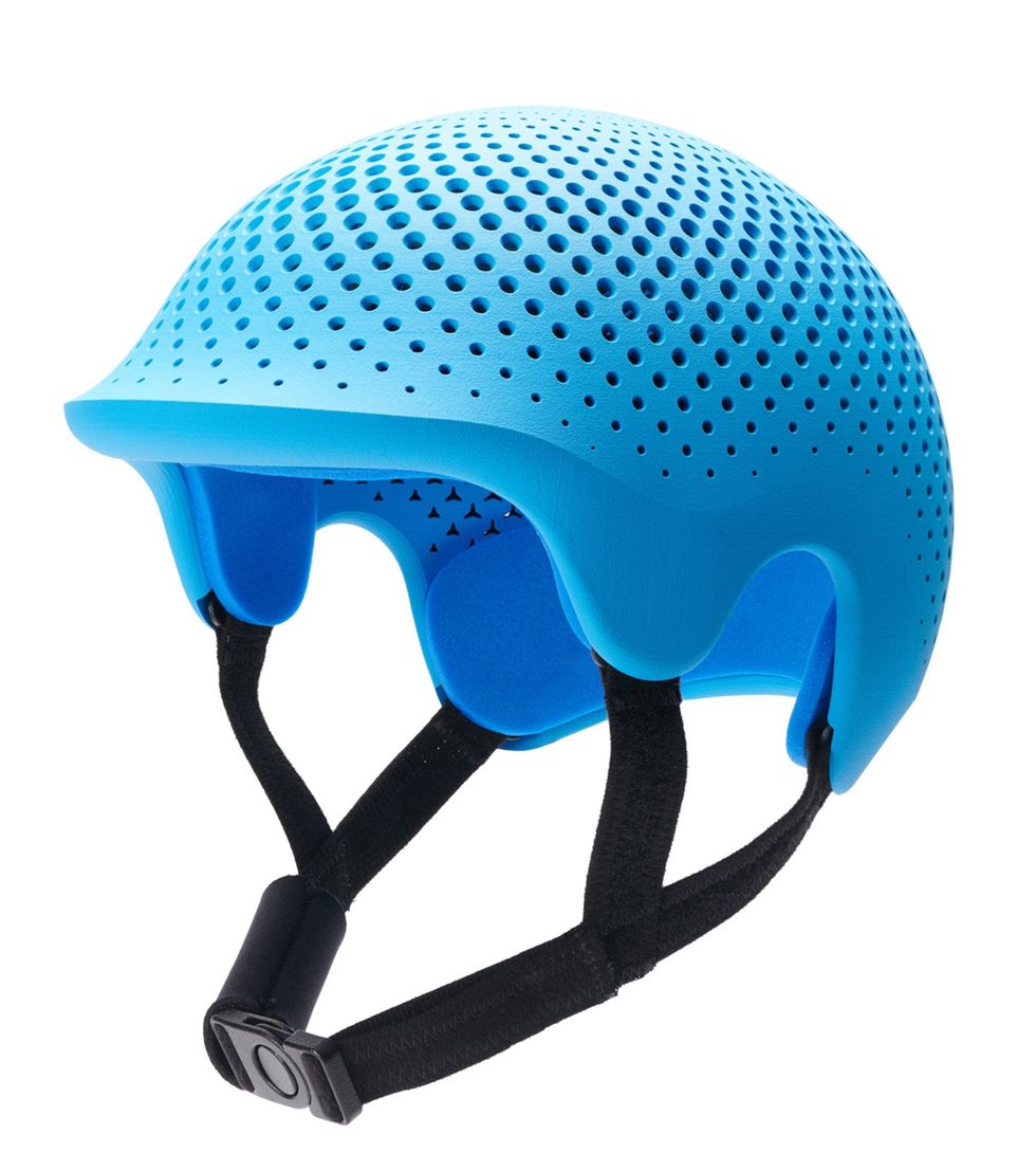
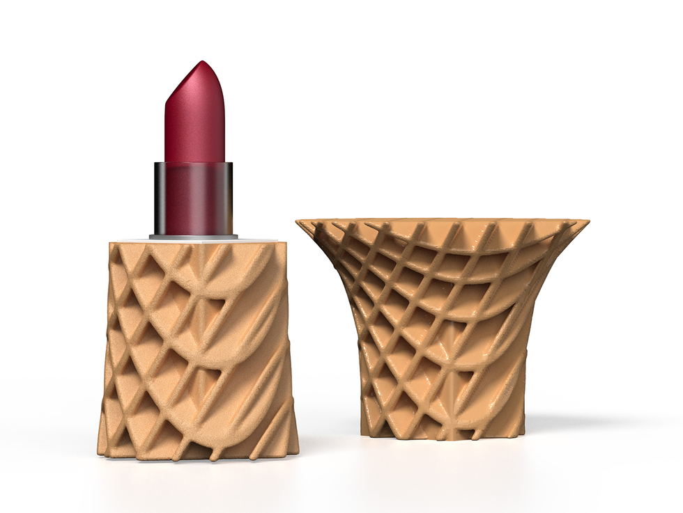
Photos of 3D printed objects Invent Medical—a Czech Republic startup partnered with HP—custom printed this helmet for correcting head-shape deformities [top]. An HP Jet Fusion 5200 printed this lipstick holder [bottom].Top: Invent Medical/HP; bottom: YOO Makeup/HP

In addition to printing two-dimensional pages and building one-dimensional molecular strands, inkjet technology has for many years been used to produce three-dimensional objects. One approach is a variant of powder-bed 3D printing, in which objects are built up by fusing or binding layers of powder in the desired pattern. The inkjet printhead applies droplets of a liquid binding agent to each layer of powder in the regions that will form the finished 3D items.

The HP Multi Jet Fusion (MJF) line of 3D printers extends this approach by depositing two types of ink: One is a binding promoter and the other a detailing agent, which is applied at the edges of the pattern to prevent the promoter from bleeding into the surrounding powder. A printhead carrying a wide array of inkjet nozzles dispenses these inks, and the array is quickly followed by a lighting bar to heat the powder, fusing it in the regions where the binding promoter is present. A fresh layer of powder is then spread over the entire printing area in readiness for the next cycle of the process. At the end, compressed air and a vacuum hose remove the unfused powder to reveal the completed 3D objects. The HP MJF printers perform this in a volume of up to 38 by 28 by 38 cm.
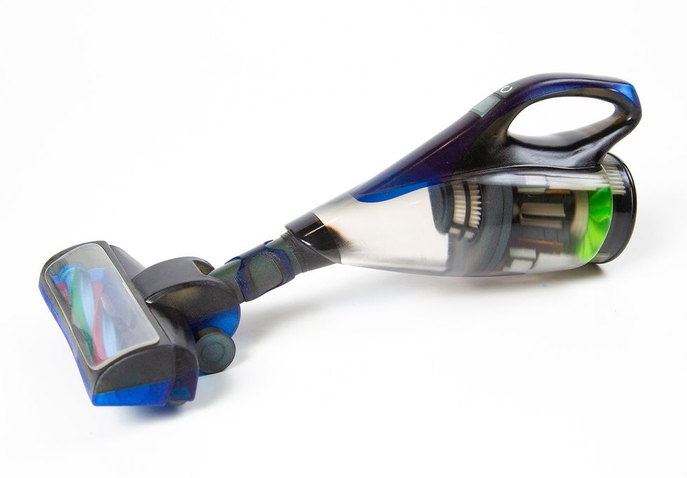
Photo of a 3D printed vacuum. This model of a handheld vacuum cleaner with colored, translucent, and transparent parts was printed in one piece on a Mimaki inkjet 3D printer.Mimaki Engineering Co.

A quite different approach has been taken by Mimaki Engineering Co. of Japan, which has introduced 3D printers with piezoelectric inkjet heads that dispense droplets of resin. The resins are photopolymers that are cured by ultraviolet light-emitting diodes after each layer is printed. Instead of using a powder bed that fills the entire build area, the printer deposits the resins on top of the growing structure. To deal with steep overhangs—such as an outstretched arm of a figurine—one of the resins produces a water-soluble material, which is used to build supports where needed. After the build is finished, these supports can be dissolved away.

Seven other resins provide colors that can include CMYK—the familiar cyan, magenta, yellow, and black inks of consumer inkjet printers—as well as white and clear, for a total of 10 million color combinations, comparable to the color depth that the human eye can discriminate. The resulting parts can combine solid color, colored transparency and translucency, and colorless transparency.

The printer provides a volume for building that measures 51 by 51 by 30 cm. Unlike with a powder-bed machine, small test parts can be made without filling the entire volume. In general, however, the Mimaki approach is slower than that of the HP MJF because it uses smaller printheads instead of a wide one that can cross the entire area in one sweep.

Inkjet’s Future

Inkjet printing’s strength is the ability to pattern various inks over large areas in short, rapid production runs at a reasonable cost. It cannot generally compete with standard high-volume production approaches, because those will usually be cheaper. Thus, a car enthusiast, for instance, may embrace 3D inkjet printing to make bespoke parts for repairs or other tinkering, but a high-volume car-parts manufacturer is not going to introduce such printers to its factory lines. Similarly, a company may build individual figurines from a customer’s design, printed by 3D inkjet, but the same technique won’t be economical for mass-producing models of the latest superhero. With many potential applications, it isn’t clear if there is a niche where the inkjet approach will win.

An example is the use of 3D inkjet printing for personalized medicine. The idea is to produce tablets of a medication customized for a specific patient. Such personalized pills can include simple fine-tuning of the dose for an individual, as well as adjustments to the drug’s release rate—from very rapid to slow and sustained—through modifications to the binding agents and structure of the tablet. Rather than juggling multiple medications on a complicated schedule each day, a patient could take a single daily polypill—a 3D-printed tablet containing multiple medications, each with a different rate of release.

Researchers are exploring how to adapt existing 3D printing techniques, including inkjet, to make these personalized medications. Inkjet systems are particularly suited for printing drugs in the form of thin films, such as transdermal patches to be applied to the skin and buccal films to be held in the cheek, where drugs can pass directly to the bloodstream without first going through the digestive system.
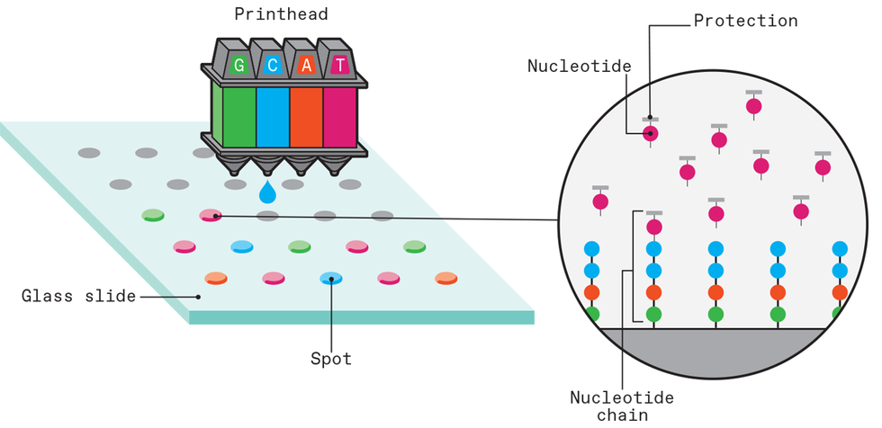
Diagram illustrating use of inkjet to build a DNA microarray. A DNA microarray can be fabricated using an inkjet system to build custom-designed strands of DNA at each spot of the array. The printhead delivers a droplet of “ink” [left] containing modified monomers of one nucleotide [G, C, A, or T] to each spot. On the first print cycle, these monomers attach to the chemically treated glass surface. On subsequent print runs [right], a single monomer joins on the end of each growing DNA strand. Each monomer includes a protective cap to prevent other monomers from joining. Additional processes [not depicted here] wash away the nucleotide ink, apply a catalyst to complete the monomer bonding, and strip away the protective caps in preparation for the next printing step.Chris Philpot

These printed personalized medicines, however, would be expensive compared to fixed doses rolling off standard high-volume production lines. Thus the technique is likely to be reserved for relatively rare conditions.

Another potential application of 3D inkjet printing is in the fabrication of advanced lithium-ion batteries. The charging and discharging of these batteries relies on lithium ions moving from the battery’s electrodes to its electrolyte and back again, in the process releasing or absorbing electrons that produce the current flow. The energy-storage density of the standard electrode design can be increased by using thicker electrodes, but this compromises the power density—the rate of energy release—because a smaller proportion of the electrode is in close contact with the electrolyte.

A 3D inkjet could build electrodes with a detailed microstructure that allows the electrolyte to penetrate throughout the electrode volume. This could boost the ability of the active lithium ions and electrons to reach the entire electrode efficiently even when the electrode is larger, thereby increasing the energy storage and power density in tandem. For this vision to become a reality, however, researchers will need to learn more about how to formulate the “inks” for printing these electrodes: What are the best particle sizes and solvents to make an ink with fluid properties suitable for use in an inkjet system and that will produce stable printed structures with good electrochemical properties?

We think it is unlikely, however, that inkjet printing could compete with high-volume manufacturing on price. Inkjet printing of prototypes, on the other hand, may uncover an optimal battery design that can then be adapted for production by conventional techniques.

Inkjet systems have been demonstrated for a wide variety of applications beyond what we have discussed above: Living cells can be printed, for instance, to form tissue structures for in vitro experiments. MEMS such as microscopic motors have been printed using inks containing nanoparticles of gold and silver as conductors and resin-based inks to act as insulators. Flexible sensors for health care monitoring have been printed using an electrically conducting polymer that responds to temperature differentials. And then there are all the ways inkjets are used to create images on media other than office printouts, such as printing of textiles, inkjet robots to apply custom automotive paint jobs, and the “GiclĂ©e” printing of fine art using archival-quality inks and substrates.

Each of these applications is like a colored dot on the vast canvas of human technology and activity. And while the dots from inkjets, powered by MEMS, may be only a single color among many others on that metaphorical page, the picture would be very different without them.

Reference: https://ift.tt/Jybuln9

Reach Your Space Goals With High-Bandwidth Devices


This sponsored article is brought to you by Avnet and AMD.

The use of artificial intelligence (AI) in image processing has brought about significant advancements in the exploration of space and our own Earth. In space applications, images are captured using various instruments, such as telescopes, satellites, and rovers. However, processing large amounts of data can be time-consuming and require significant computational power. This is where AI and powerful processors come in.

AI algorithms, with the support of industry-leading processors, can handle large amounts of data quickly and accurately. They can also learn from previous data to improve their analysis of new data. AI algorithms can be trained to recognize patterns in images, classify them, and identify anomalies.

One of the main applications of AI in image processing for space is in the detection and classification of objects. For example, AI can be used to detect and classify asteroids or other celestial bodies. This information can be used to determine the trajectory of these objects and their potential impact on Earth. AI can also identify and classify space debris, which is a growing concern for space missions.

Combining AI and Cutting-Edge Processors

This also applies to objects closer to home. Earth-observing instruments rely on AI algorithms and processors to collect large amounts of information each day. However, transforming that raw data into information that can be acted upon is the real challenge, especially when instruments need to determine which data points are the most important.

There are wildfires, harmful algal blooms, volcanic eruptions, and heavy snowfalls. If we can observe these events better, we will have an opportunity to react by making the world safer and cleaner for humans.

AI and cutting-edge processors can also be used to improve the resolution of images captured by telescopes and satellites. By analyzing the data captured by these instruments, AI algorithms can remove noise and improve the clarity of the images. This can help scientists better understand the structure and composition of celestial bodies as well as detect water on other planets. By analyzing the spectral signatures of the surface of these planets, AI algorithms can detect the presence of water. This information can be used to determine if these planets are habitable. AI can also identify other important minerals and resources on these planets.

AMD processors and advancements in AI are enabling limitless possibilities for space exploration.

AMD processors are transforming image processing for space applications with high throughput, low latency, and unlimited in-orbit reconfigurability. This enables scientists to analyze large amounts of data quickly and accurately. When paired with AI algorithms, the AMD KintexTM UltraScale, AMD VersalTM SoCs, and AMD VirtexTM devices can detect and classify objects, improve the resolution of images, detect the presence of water and other imperative resources on other planets. AMD processors and advancements in AI are enabling limitless possibilities for space exploration.

Learn how Avnet and AMD are enabling the next generation of space applications that bring AI, imaging and more together to help humans explore beyond our limits. We’ve compiled several case studies that illustrate these cutting-edge technologies in real-world applications. Click here to explore how.

Reference: https://ift.tt/PqW0ICV

Saturday, March 23, 2024

We Need to Decarbonize Software


Software may be eating the world, but it is also heating it.

In December 2023, representatives from nearly 200 countries gathered in Dubai for COP28, the U.N.’s climate-change conference, to discuss the urgent need to lower emissions. Meanwhile, COP28’s website produced 3.69 grams of carbon dioxide (CO2) per page load, according to the website sustainability scoring tool Ecograder. That appears to be a tiny amount, but if the site gets 10,000 views each month for a year, its emissions would be a little over that of a one-way flight from San Francisco to Toronto.

This was not inevitable. Based on Ecograder’s analysis, unused code, improperly sized images, and third-party scripts, among other things, affect the COP28 website’s emissions. These all factor into the energy used for data transfer, loading, and processing, consuming a lot of power on users’ devices. Fixing and optimizing these things could chop a whopping 93 percent from the website’s per-page-load emissions, Ecograder notes.

While software on its own doesn’t release any emissions, it runs on hardware in data centers and steers data through transmission networks, which account for about 1 percent of energy-related greenhouse gas emissions each. The information and communications technology sector as a whole is responsible for an estimated 2 to 4 percent of global greenhouse gas emissions. By 2040, that number could reach 14 percent—almost as much carbon as that emitted by air, land, and sea transport combined.

Within the sphere of software, artificial intelligence has its own sustainability issues. AI company Hugging Face estimated the carbon footprint of its BLOOM large language model across its entire life cycle, from equipment manufacturing to deployment. The company found that BLOOM’s final training emitted 50 tonnes of CO2—equivalent to about a dozen flights from New York City to Sydney.

Green software engineering is an emerging discipline consisting of best practices to build applications that reduce carbon emissions. The green software movement is fast gaining momentum. Companies like Salesforce have launched their own software sustainability initiatives, while the Green Software Foundation now comprises 64 member organizations, including tech giants Google, Intel, and Microsoft. But the sector will have to embrace these practices even more broadly if they are to prevent worsening emissions from developing and using software.

What Is Green Software Engineering?

The path to green software began more than 10 years ago. The Sustainable Web Design Community Group of the World Wide Web Consortium (W3C) was established in 2013, while the Green Web Foundation began in 2006 as a way to understand the kinds of energy that power the Internet. Now, the Green Web Foundation is working toward the ambitious goal of a fossil-free Internet by 2030.

Green Software Resources


  • The Green Software Foundation offers a catalog of green software patterns for AI, the cloud, and the Web.
  • The W3C’s Sustainable Web Design Community Group released a draft of its Web sustainability guidelines, with both tactical and technical recommendations for business and product strategy, user-experience design, Web development, and hosting and infrastructure. The draft guidelines also include impact and effort ratings to give software engineers an idea of the level of difficulty in terms of implementation and the level of impact in terms of sustainability.

“There’s an already existing large segment of the software-development ecosystem that cares about this space—they just haven’t known what to do,” says Asim Hussain, chairperson and executive director of the Green Software Foundation and former director of green software and ecosystems at Intel.

What to do, according to Hussain, falls under three main pillars: energy efficiency, or using less energy; hardware efficiency, or using fewer physical resources; and carbon-aware computing, or using energy more intelligently. Carbon-aware computing, Hussain adds, is about doing more with your applications during the periods when the electricity comes from clean or low-carbon sources—such as when wind and solar power are available—and doing less when it doesn’t.

The Case for Sustainable Software

So why should programmers care about making their software sustainable? For one, green software is efficient software, allowing coders to cultivate faster, higher-quality systems, says Kaspar Kinsiveer, a team lead and sustainable-software strategist at the software-development firm Helmes.

These efficient systems could also mean lower costs for companies. “One of the main misconceptions about green software is that you have to do something extra, and it will cost extra,” Kinsiveer says. “It doesn’t cost extra—you just have to do things right.”


Green software is efficient software, allowing coders to cultivate faster, higher-quality systems.


Other motivating factors, especially on the business side of software, are the upcoming legislation and regulations related to sustainability. In the European Union, for instance, the Corporate Sustainability Reporting Directive requires companies to report more on their environmental footprint, energy usage, and emissions, including the emissions related to the use of their products.

Yet other developers may be motivated by the climate crisis itself, wanting to play their part in fostering a habitable planet for the coming generations. And software engineers have tremendous influence on the actual purpose and emissions of what they build.

“It’s not just lines of code. Those lines have an impact on human beings,” says June Sallou, a postdoctoral researcher specializing in sustainable-software engineering at the Delft University of Technology, in the Netherlands. Because of AI’s societal impact in particular, she adds, developers have a responsibility to ensure that what they’re creating isn’t damaging the environment.

Building Greener Websites and Apps

The makers of COP28’s website could have taken a page from directories like Lowwwcarbon, which highlights examples of existing low-carbon websites. The company website of the Netherlands-based Web design and branding firm Tijgerbrood, for instance, emits less than 0.1 grams of carbon per page view.

Creating sustainable websites like Tijgerbrood’s is a team effort that involves different roles—from business analysts who define software requirements to designers, architects, and those in charge of operations—and includes green practices that can be applied at each stage of the software-development process.

Tips for Greener Websites and Apps


First, analysts will have to consider if the feature, app, or software they’re designing should even be developed in the first place. Tech is often about creating the next new thing, but making software sustainable also entails decisions on what not to build, and that may require a shift in mind-set.

The design stage is all about choosing efficient algorithms and architectures. “Think about sustainability before going into the solution—and not after,” says Chiara Lanza, a researcher at the Sustainable AI unit of the Centre Tecnològic de Telecomunicacions de Catalunya, in Barcelona.

During the development stage, programmers need to focus on optimizing code. “We need the overall amount of energy we’re using to run software to go down. Some of that will come from writing [code] efficiently,” says Hannah Smith, a sustainable digital tech consultant and director of operations at the Green Web Foundation.

Tijgerbrood’s website optimized the company’s code by using low-resolution images and modern image formats, loading animations only when a user scrolls them into view, and removing unnecessary code. These techniques help speed up data transfer, loading, and processing on a user’s device. The website also uses minimal JavaScript. “When a user loads a website [with] a lot of JavaScript, it causes them to use a lot more energy on their own device because their device is having to do all the work of reading the JavaScript and running [it],” explains Smith.

When it comes to operations, one of the most impactful actions you can take is to select a sustainable Web hosting or cloud-computing provider. The Green Web Foundation has a tool to check if your website runs on green energy, as well as a directory of hosting providers powered by renewable energy. You can also ask your hosting provider if you can scale how your software runs in the cloud so that peak usage is powered by green energy or pause or switch off certain services during nonpeak hours.

AI the Green Way


Programmers can apply green software strategies when developing AI as well. Trimming training data is one of the major ways to make AI systems greener. Starting with data collection and preprocessing, it’s worth thinking about how much data is really needed to do the job. It may pay to clean the dataset to remove unnecessary data, or select only a subset of the dataset for training.

“The larger your dataset is, the more time and computation it will take for the algorithm to go through all the data,” hence using up more energy, says Sallou.

For instance, in a study of six different AI algorithms that detect SMS spam messages, Sallou and her colleagues found that the random forest algorithm, which combines the output of a collection of decision trees to make a prediction, was the most energy-greedy algorithm. But reducing the size of the training dataset to 20 percent—only 1,000 data points out of 5,000—dropped the energy consumption of training by nearly 75 percent, with only a 0.06 percent loss in accuracy.

Choosing a greener algorithm could also save carbon. Tools like CodeCarbon and ML CO2 Impact can help make the choice by estimating the energy usage and carbon footprint of training different AI models.

Tips for Greener AI


Tools for Measuring Software’s Carbon Footprint

To write green code, developers need a way of measuring the actual carbon emissions across a system’s entire life cycle. It’s a complex feat, given the myriad processes involved. If we take AI as an example, its life cycle encompasses raw material extraction, materials manufacturing, hardware manufacturing, model training, model deployment, and disposal—and not all of these stages have available data.

“We don’t understand huge parts of the ecosystem at the moment, and access to reliable data is tough,” Smith says. The biggest need, she adds, is “open data that we can rely on and trust” from big tech data-center operators and cloud providers like Amazon, Google, and Microsoft.

Until that data surfaces, a more practical approach would be to measure how much power software consumes. “Just knowing the energy consumption of running a piece of software can impact how software engineers can improve the code,” Sallou says.

Developers themselves are heeding the call for more measurement, and they’re building tools to meet this demand. The W3C’s Sustainable Web Design Community Group, for instance, plans to provide a test suite to measure the impacts of implementing its Web sustainability guidelines. Similarly, the Green Software Foundation wrote a specification to calculate the carbon intensity of software systems. For accurate measurements, Lanza suggests isolating the hardware in which a system runs from any other operations and to avoid running any other programs that could influence measurements.

Other tools developers can use to measure the impact of green software engineering practices include dashboards that give an overview of the estimated carbon emissions associated with cloud workloads, such as the AWS Customer Carbon Footprint Tool and Microsoft’s Azure Emissions Impact Dashboard; energy profilers or power monitors like Intel’s Performance Counter Monitor; and tools that help calculate the carbon footprint of websites, such as Ecograder, Firefox Profiler, and Website Carbon Calculator.

Green Software Measurement Tools 


Developers can use these tools to measure the impact of green software engineering practices.

AI

Estimate the energy usage and carbon footprint of training AI models with these tools.

carbontracker
experiment-impact-tracker
ML CO2 Impact

Cloud

These dashboards give an overview of the estimated carbon emissions associated with cloud workloads.
AWS Customer Carbon Footprint Tool
Google Cloud Carbon Footprint
Microsoft Azure Emissions Impact Dashboard
Cloud Carbon Footprint (free, open source, provider agnostic)

Code

Integrate emissions estimation at the code level using these tools.
Carbon-Aware SDK
CodeCarbon
Impact Framework

Middleware

These energy profilers or power monitors provide APIs (application programming interfaces) to measure power consumption of apps or track energy metrics of processors.
Intel’s Performance Counter Monitor
PowerAPI

Web

These tools help calculate the carbon footprint of websites.
Are my third parties green?
CO2.js
Ecograder
Firefox Profiler
Website Carbon Calculator


The Future Is Green

Green software engineering is growing and evolving, but we need more awareness to help the discipline to become more widespread. This is why, in addition to its Green Software for Practitioners course, the Green Software Foundation aims to create more training courses, some of which may even lead to certifications. Likewise, Sallou coteaches a graduate course in sustainable software engineering, whose syllabus is open and can be used as a foundation for anyone looking to build a similar course. Providing this knowledge to students early on, she says, could ensure they bring it to their workplaces as future software engineers.

In the realm of artificial intelligence, Navveen Balani, an AI expert and Google Cloud Certified Fellow who also serves on the Green Software Foundation’s steering committee, notes that AI could inherently include green AI principles in the coming years, much like how security considerations are now an integral part of software development. “This shift will align AI innovation with environmental sustainability, making green AI not just a specialty but an implied standard in the field,” he says.

As for the Web, Smith hopes the Green Web Foundation will cease to exist by 2030. “Our dream as an organization is that we’re not needed, we meet our goal, and the Internet is green by default,” she says.

Kinsiveer has observed that in the past, software had to be optimized and built well because hardware then was lacking. As hardware performance and innovation leveled up, “the quality of programming itself went down,” he says. But now, the industry is coming full circle, going back to its efficiency roots and adding sustainability to the mix.

“The future is green software,” Kinsiveer says. “I cannot imagine it any other way.”

Reference: https://ift.tt/BVrQNy9

Friday, March 22, 2024

Video Friday: Project GR00T


Video Friday is your weekly selection of awesome robotics videos, collected by your friends at IEEE Spectrum robotics. We also post a weekly calendar of upcoming robotics events for the next few months. Please send us your events for inclusion.

Eurobot Open 2024: 8–11 May 2024, LA ROCHE-SUR-YON, FRANCE
ICRA 2024: 13–17 May 2024, YOKOHAMA, JAPAN
RoboCup 2024: 17–22 July 2024, EINDHOVEN, NETHERLANDS

Enjoy today’s videos!

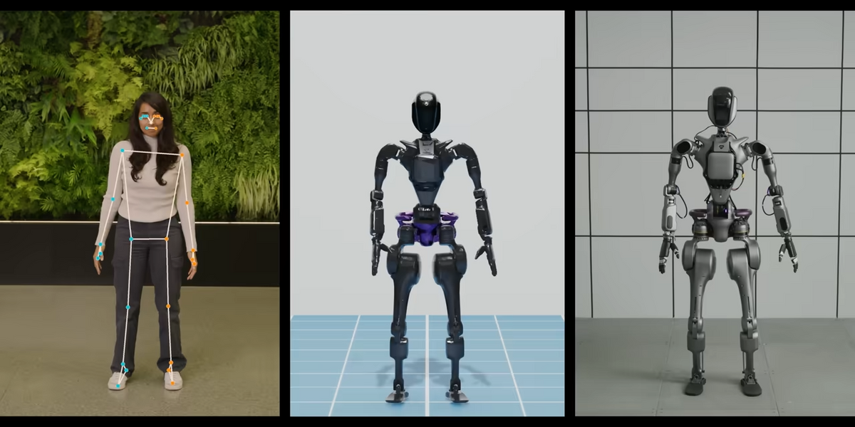
See NVIDIA’s journey from pioneering advanced autonomous vehicle hardware and simulation tools to accelerated perception and manipulation for autonomous mobile robots and industrial arms, culminating in the next wave of cutting-edge AI for humanoid robots.

[ NVIDIA ]

In release 4.0, we advanced Spot’s locomotion abilities thanks to the power of reinforcement learning. Paul Domanico, Robotics Engineer at Boston Dynamics talks through how Spot’s hybrid approach of combining reinforcement learning with model predictive control creates an even more stable robot in the most antagonistic environments.

[ Boston Dynamics ]

We’re excited to share our latest progress on teaching EVEs general-purpose skills. Everything in the video is all autonomous, all 1X speed, all controlled with a single set of neural network weights.

[ 1X ]

What I find interesting about the Unitree H1 doing a standing flip is where it decides to put its legs.

[ Unitree ]

At the MODEX Exposition in March of 2024, Pickle Robot demonstrated picking freight from a random pile similar to what you see in a messy truck trailer after it has bounced across many miles of highway. The piles of boxes were never the same and the demonstration was run live in front of crowds of onlookers 25 times over 4 days. No other robotic trailer/container unloading system has yet to demonstrate this ability to pick from unstructured piles.

[ Pickle ]

RunRu is a car-like robot, a robot-like car, with autonomy, sociability, and operability. This is a new type of personal vehicle that aims to create a “Jinba-Ittai” relationship with its passengers, who are not only always assertive, but also sometimes whine.

[ ICD-LAB ]

Verdie went to GTC this year and won the hearts of people but maybe not the other robots.

[ Electric Sheep ]

The “DEEPRobotics AI+” merges AI capabilities with robotic software systems to continuously boost embodied intelligence. The showcased achievement is a result of training a new AI and software system.

[ DEEP Robotics ]

If you want to collect data for robot grasping, using Stretch and a pair of tongs is about as affordable as it gets.

[ Hello Robot ]

The real reason why Digit’s legs look backwards is so that it doesn’t bang its shins taking GPUs out of the oven.

Meanwhile, some of us can bake our GPUs without even needing an oven.

[ Agility ]

P1 is LimX Dynamics’ innovative point-foot biped robot, serving as an important platform for the systematic development and modular testing of reinforcement learning. It is utilized to advance the research and iteration of basic biped locomotion abilities. The success of P1 in conquering forest terrain is a testament to LimX Dynamics’ systematic R&D in reinforcement learning.

[ LimX ]

And now, this.

[ Suzumori Endo Lab ]

Cooking in kitchens is fun. BUT doing it collaboratively with two robots is even more satisfying! We introduce MOSAIC, a modular framework that coordinates multiple robots to closely collaborate and cook with humans via natural language interaction and a repository of skills.

[ Cornell ]

neoDavid is a Robust Humanoid with Dexterous Manipulation Skills, developed at DLR. The main focus in the development of neoDavid is to get as close to human capabilities as possible—especially in terms of dynamics, dexterity and robustness.

[ DLR ]

Welcome to our customer spotlight video series where we showcase some of the remarkable robots that our customers have been working on. In this episode we showcase three Clearpath Robotics UGVs that our customers are using to create robotic assistants for three different applications.

[ Clearpath ]

This video presents KIMLAB’s new three-fingered robotic hand, featuring soft tactile sensors for enhanced grasping capabilities. Leveraging cost-effective 3D printing materials, it ensures robustness and operational efficiency.

[ KIMLAB ]

Various perception-aware planning approaches have attempted to enhance the state estimation accuracy during maneuvers, while the feature matchability among frames, a crucial factor influencing estimation accuracy, has often been overlooked. In this paper, we present APACE, an Agile and Perception-Aware trajeCtory gEneration framework for quadrotors aggressive flight, that takes into account feature matchability during trajectory planning.

[ Paper ] via [ HKUST ]

In this video, we see Samuel Kunz, the pilot of the RSL Assistance Robot Race team from ETH Zurich, as he participates in the CYBATHLON Challenges 2024. Samuel completed all four designated tasks—retrieving a parcel from a mailbox, using a toothbrush, hanging a scarf on a clothesline, and emptying a dishwasher—with the help of an assistance robot. He achieved a perfect score of 40 out of 40 points and secured first place in the race, completing the tasks in 6.34 minutes.

[ CYBATHLON ]

Florian Ledoux is a wildlife photographer with a deep love for the Arctic and its wildlife. Using the Mavic 3 Pro, he steps onto the ice ready to capture the raw beauty and the stories of this chilly, remote place.

[ DJI ]

Reference: https://ift.tt/CKk1oVd

6G Terahertz Devices Demand 3D Electronics


Smartphones have a scaling problem. Specifically, the radiofrequency (RF) filters that every phone—and every wireless device in general—uses to extract information from isolated wireless signals are too big, too flat, and too numerous. And without these filters, wireless communications simply wouldn’t work at all.

“They are literally the entire backbone of wireless systems,” says Roozbeh Tabrizian, a researcher at the University of Florida in Gainesville.

So Tabrizian and other researchers at the University of Florida have now developed an alternative three-dimensional RF filter that can save space in smartphones and IoT devices. If these 3D filters one day replace bulky stacks of 2D filters, it would leave more room for other components, such as batteries. They could also make it easier to push wireless communications into terahertz frequencies, an important spectrum range being researched for 6G cellular technologies.

“Very soon, we’ll have trillions of devices connected to wireless networks, and you need new bands, you just need a whole range of frequencies and a whole range of filters.” —Roozbeh Tabrizian, University of Florida

The filters currently used by wireless devices are called planar piezoelectric resonators. Each resonator is a different thickness—a resonator’s specific thickness is directly tied to the band of wireless frequencies that resonator responds to. Any wireless device that relies on multiple bands of spectrum—increasingly commonplace today—requires more and more of these flat resonators.

But planar resonator technology has revealed a number of weaknesses as wireless signals proliferate and as the spectrum those signals relies on broadens. One is that it’s getting more difficult to make the filters thin enough for the new swathes of spectrum that wireless researchers are interested in harnessing for next-gen communications. Another involves space. It’s proving increasingly challenging to cram all of the signal filters needed into devices.

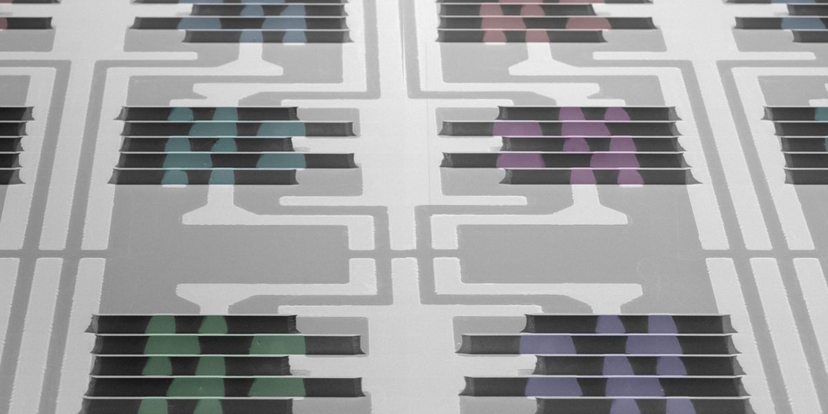
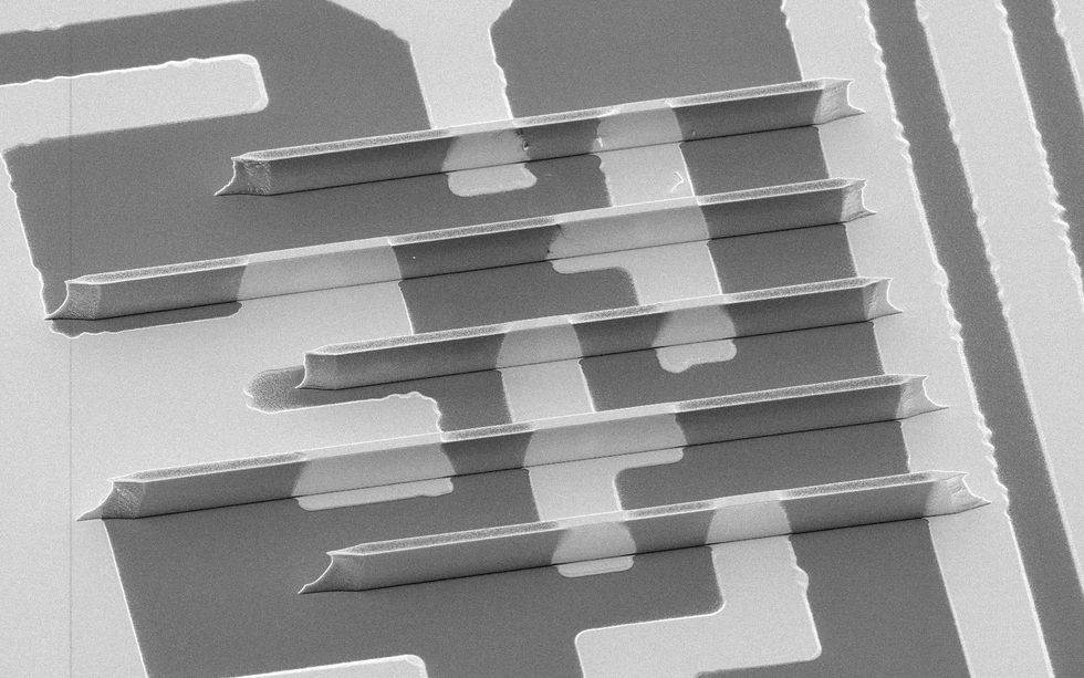
A top-down image of five silver-colored vertical fins of different lengths rising up from a gray surface. The vertical fins for ferroelectric-gate fin resonators can be constructed in the same manner as FinFET semiconductors.Faysal Hakim/Roozbeh Tabrizian/University of Florida


“Very soon, we’ll have trillions of devices connected to wireless networks, and you need new bands, you just need a whole range of frequencies and a whole range of filters,” says Tabrizian. “If you open up a cell phone, there are five or six specific frequencies, and that’s it. Five or six frequencies cannot handle that. It’s as if you have five or six streets, and now you want to accommodate the traffic of a city of 10 million people.”

To make the switch to a 3D filter, Tabrizian and his fellow researchers took a page from another industry that made the jump to the third dimension: semiconductors. When, in the continuous quest to shrink down chip sizes, it seemed like the industry might finally be hitting end of the road, a new approach that raised electron channels above the semiconductor substrate breathed new life into Moore’s Law. The chip design is called FinFET (for “fin field-effect transistor,” where “fin” refers to the shark-fin-like vertical electron channel).

“The fact that we can change the width of the fin plays a huge role in making the technology much more capable.” —Roozbeh Tabrizian, University of Florida

“We definitely got inspired [by FinFETS],” says Tabrizian. “The fact that planar transistors were converted to fins was just to make sure the effective size of the transistor was smaller while having the same active area.”

Despite taking inspiration from FinFETs, Tabrizian says there are some fundamental differences in the way the vertical fins need to be implemented for RF filters, compared to chips. “If you think of FinFETs, all the fins are nearly the same width. People are not changing the dimension of the of the fin.”

Not so for filters, which must have fins of different widths. That way, each fin on the filter can be tuned to different frequencies, allowing one 3D filter to process multiple spectrum bands. “The fact that we can change the width of the fin plays a huge role in making the technology much more capable,” says Tabrizian.

Tabrizian’s group have already manufactured multiple three-dimensional filters, called ferroelectric-gate fin (FGF) resonators, that spanned frequencies between 3 and 28 GHz. They also constructed a spectral processor comprised of six integrated FGF resonators that covered frequencies between 9 and 12 GHz (By way of comparision, 5G’s coveted midband spectrum falls between 1 and 6 GHz). The researchers published their work in January in Nature Electronics.

It’s still early days for 3D filter development, and Tabrizian acknowledges that the road ahead is long. But again taking inspiration from FinFETs, he sees a clear path of development for FGF resonators. “The good news is we can already guess what a lot of these challenges are by looking at FinFET technology,” he says.

Incorporating FGF resonators into commercial devices someday will require solving several manufacturing problems, such as figuring out how to increase the density of fins on the filter and improving the electrical contacts. “Fortunately, since we already have FinFETs going through a lot of these answers, the manufacturing part is already being addressed,” Tabrizian says.

One thing the research group is already working on is the process design kit, or PDK, for FGF resonators. PDKs are commonplace in the semiconductor industry, and they function as a kind of guidebook for designers to fabricate chips based on components detailed by a chip foundry.

Tabrizian also sees a lot of potential for future manufacturing to integrate FGF resonators and semiconductors into one component, given their similarities in design and fabrication. “It’s human innovation and creativity to come up with new types of architectures, which may revolutionize the way that we think about having resonators and filters and transistors.”

Reference: https://ift.tt/xToicSn

Thursday, March 21, 2024

Never-before-seen data wiper may have been used by Russia against Ukraine


Never-before-seen data wiper may have been used by Russia against Ukraine

Enlarge (credit: Getty Images)

Researchers have unearthed never-before-seen wiper malware tied to the Kremlin and an operation two years ago that took out more than 10,000 satellite modems located mainly in Ukraine on the eve of Russia’s invasion of its neighboring country.

AcidPour, as researchers from security firm Sentinel One have named the new malware, has stark similarities to AcidRain, a wiper discovered in March 2022 that Viasat has confirmed was used in the attack on its modems earlier that month. Wipers are malicious applications designed to destroy stored data or render devices inoperable. Viasat said AcidRain was installed on more than 10,000 Eutelsat KA-SAT modems used by the broadband provider seven days prior to the March 2022 discovery of the wiper. AcidRain was installed on the devices after attackers gained access to the company’s private network.

Sentinel One, which also discovered AcidRain, said at the time that the earlier wiper had enough technical overlaps with malware the US government attributed to the Russian government in 2018 to make it likely that AcidRain and the 2018 malware, known as VPNFilter, were closely linked to the same team of developers. In turn, Sentinel One’s report Thursday noting the similarities between AcidRain and AcidPour, provides evidence that AcidPour was also created by developers working on behalf of the Kremlin.

Read 10 remaining paragraphs | Comments

Reference : https://ift.tt/VkNQDSW

Hackers can extract secret encryption keys from Apple’s Mac chips


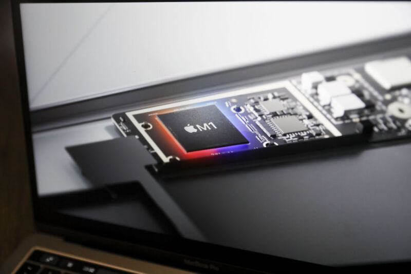
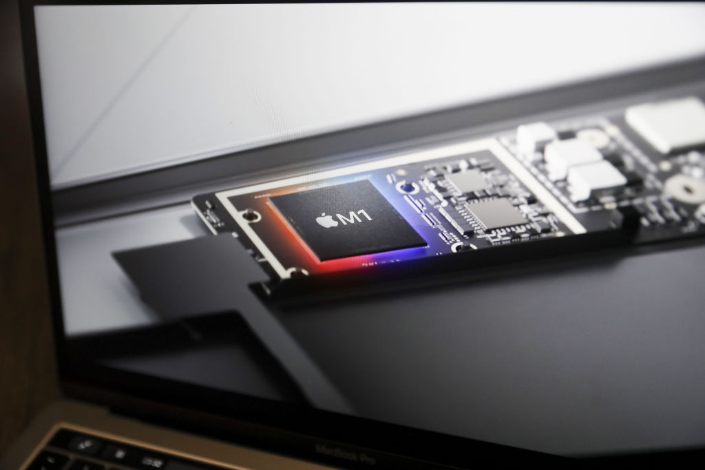
Apple's M1 chip.

Enlarge / Apple's M1 chip. (credit: Photographer: Daniel Acker/Bloomberg via Getty Images)

A newly discovered vulnerability baked into Apple’s M-series of chips allows attackers to extract secret keys from Macs when they perform widely used cryptographic operations, academic researchers have revealed in a paper published Thursday.

The flaw—a side channel allowing end-to-end key extractions when Apple chips run implementations of widely used cryptographic protocols—can’t be patched directly because it stems from the microarchitectural design of the silicon itself. Instead, it can only be mitigated by building defenses into third-party cryptographic software that could drastically degrade M-series performance when executing cryptographic operations, particularly on the earlier M1 and M2 generations. The vulnerability can be exploited when the targeted cryptographic operation and the malicious application with normal user system privileges run on the same CPU cluster.

Beware of hardware optimizations

The threat resides in the chips’ data memory-dependent prefetcher, a hardware optimization that predicts the memory addresses of data that running code is likely to access in the near future. By loading the contents into the CPU cache before it’s actually needed, the DMP, as the feature is abbreviated, reduces latency between the main memory and the CPU, a common bottleneck in modern computing. DMPs are a relatively new phenomenon found only in M-series chips and Intel's 13th-generation Raptor Lake microarchitecture, although older forms of prefetchers have been common for years.

Read 19 remaining paragraphs | Comments

Reference : https://ift.tt/K12nfFq

Targeted ads delivered 0-click exploits to install mercenary malware

<p>Researchers say that mercenary hackers laced ads with zero-click exploits that installed sophisticated...