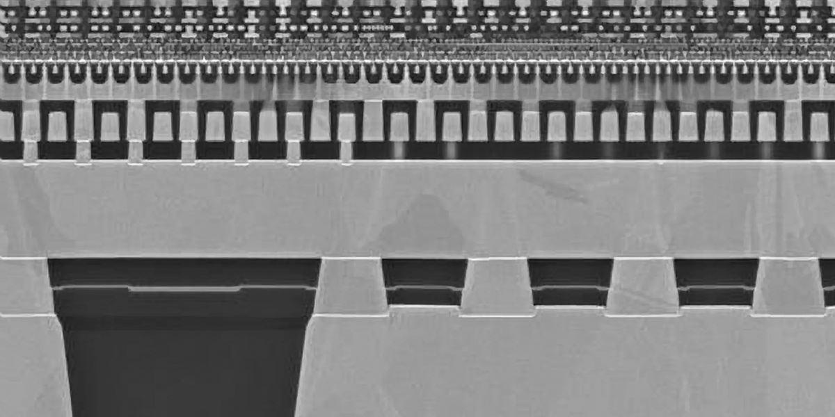

For the past five years, Intel has lagged behind Taiwan Semiconductor Manufacturing Co. and Samsung in advanced chip manufacturing. Now, in an attempt to regain the lead, the company is making a bold—and risky—move, introducing two novel technologies in its desktop and laptop Arrow Lake processor, due out in late 2024. Intel hopes to leapfrog its competitors with new transistor technology and a power-delivery system that would be the first of its kind.
Over the past two decades, Intel has led the field in making key changes to the transistor architecture, says Chris Auth, Intel’s vice president of technology development and director of advanced transistor development. The company’s chip production, however, has a more checkered past: In 2018, Intel couldn’t deliver its first 10-nanometer CPU on time, and manufacturing of the chip was postponed a year, creating a shortage of CPUs made using its 14-nm technology. In 2020 there were delays again, this time for the 7-nm node (rebranded as Intel 4). The company has been playing catch-up ever since.
RibbonFET, Intel’s nanosheet transistor, will replace today’s FinFET technology. FinFET transistors had provided CPUs with low power requirements and greater logic circuit density by wrapping the transistor’s gate around its channel region on three sides instead of just one. But as the FinFETs have scaled down in size, these devices have approached the limit of their gates’ ability to control current. Nanosheet transistors, such as Samsung’s Multi-Bridge-Channel FET, provide better control because their gates completely surround the channel region. Intel expects up to 15 percent improvement in energy efficiency with RibbonFET when it is introduced in the upcoming Intel 20A processing node—the company’s latest semiconductor manufacturing process technology. The “A” in 20A refers to the angstrom—though, like “nanometer” in the previous chip-naming convention, it no longer refers to a specific measurement in the product.
The introduction of a new power-delivery scheme—which is generally called back-side power and which Intel calls PowerVia—is a more dramatic change. “Ever since Robert Noyce made the first integrated circuit, everything’s been on the front side for interconnects,” says Auth. This will be the first time that manufacturers will use the surface on the other side of the wafer, too, separating power from processing. That decoupling is important because power and signal lines have different optimizations: While power lines perform best with low-resistance, high-gauge wires, signal lines need more space between them to ensure minimal interference.
“It’s kind of a new playground,” says Julien Ryckaert, vice president for logic technologies at Imec. The move to nanosheet technology is conventional, but Ryckaert expects opportunities for innovative new features with back-side power.
Two Technologies at Once
Intel decided to introduce both technologies simultaneously about five years ago, around the same time it lost its lead over competitors. Typically, these types of projects operate on a decade-long timeline. As Intel got closer to implementing the new transistors and power-delivery network, its executives saw that these timelines were set to intersect. So, to get ahead of its competitors and avoid waiting for the next node to introduce one or the other, the company decided to pair the technologies. Both are seen as “key linchpins” toward Intel’s ambitious goal to regain the lead in processing technology by 2025, Auth says.
“Intel used to be the conservative one,” says Dan Hutcheson, vice chair of TechInsights. Previously, TSMC was more aggressive in its risk-taking, and the company more frequently missed the mark. Now, the situation has flipped, Hutcheson explains. “It’s a very risky move to try to implement two major technology changes at once, and in the past this has often been a recipe for disaster,” he says.
Intel’s innovation needs to be delivered with reliable production to attract and maintain customers, Hutcheson adds, especially as it continues to shift its business toward a semiconductor foundry model by separating its manufacturing and product groups. In a foundry model, it’s essential that customers can trust the manufacturer, he says. Due to the long-term investment from development to delivering a product, customers are “basically betting the farm about two years out.”
Company executives are well aware of the risk they’re taking, given the setbacks and delays Intel faced with the 10-nm node. While the industry is “built on taking risks,” Auth says, “that was a case where we took on too much risk, and we’re definitely cognizant of that mistake.”
So, to reduce the risk involved in the upcoming 20A node, Intel added an internal node pairing PowerVia with the current generation of FinFET. According to test results presented in June 2023, adding PowerVia alone led to a 6 percent performance gain. This internal stepping-stone has allowed the company to test out back-side power delivery and address any issues, both in terms of process and design.
On the process side, for example, Intel needs to figure out how to properly align and link the front and back sides of the chip with nanometer-size vertical connectors called through-silicon vias that are 1/500 the size of previous connectors. Another challenge comes in maintaining the flat surfaces needed to pattern the chips when working with both sides of the silicon wafer, Auth says.
Given this need for even more precision in manufacturing, it’s worth considering the projected cost, says Mark Horowitz, a professor of electrical engineering at Stanford University. Historically, cost per transistor decreased as manufacturers scaled to better technologies. Now, these cost improvements are generally plateauing. “Transistors are not getting cheaper as fast as they used to,” Horowitz says.
Meanwhile, designers have to rethink the interconnect lines and layout. By moving the power lines to the back side of the chip with PowerVia, Auth says, “you’re undoing about seven years of front-side interconnect learning.” Engineers had to relearn how to find defects and properly dissipate heat, for example. Despite the steep learning curve, Intel anticipates significant benefits from the combination of the new technologies.
With each advance addressing an independent aspect of scaling, the new transistor and power-delivery network can be seen as complementary, according to Imec’s Ryckaert. He suspects Intel’s decision to introduce back-side power during the FinFET-to-nanosheet transition was made to entice customers, by providing a more significant benefit than either advance could deliver by itself. There may not be many future generations that will use nanosheet transistor tech. “Very rapidly, we’re going to see the saturation of nanosheet,” Ryckaert predicts.
Intel expects to be ready for manufacturing 20A in the first half of 2024. TSMC plans to begin production of chips with its N2 nanosheet technology in early 2025. Production of N2P chips—a version with back-side power delivery—is expected to begin by 2026. Samsung has already introduced nanosheet transistors in its 3-nm node in 2022 but hasn’t officially announced a timeline for implementing back-side power.
Hutcheson believes that all chipmakers are on the same path toward back-side power; Intel is just the first to take the leap. If the company pulls it off, that risk could allow it to regain the lead, he says. “There’s a lot riding on this.”
This article appears in the January 2024 print issue as “Intel Hopes to Leapfrog Its Competitors.”
Reference: https://ift.tt/OIsX3vk
No comments:
Post a Comment