
On Monday, Intel unveiled new details of the processor that will power the Aurora supercomputer, which is designed to become the one of the first U.S.-based high-performance computers (HPCs) to pierce the exaflop barrier—a billion billion high-precision floating point calculations per second. Intel Fellow Wilfred Gomes told engineers virtually attending the IEEE International Solid State Circuits Conference this week that the processor pushed Intel's 2D and 3D chiplet integration technologies to the limits.
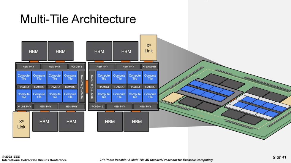
The processor, called Ponte Vecchio, is a package that combines multiple compute, cache, networking, and memory silicon tiles, or "chiplets". Each of the tiles in the package is made using different process technologies, in a stark example of a trend called heterogenous integration.
Ponte Vecchio is, among other things, a master class in 3D integration.
The result is that Intel packed 3,100 square millimeters of silicon—nearly equal to four Nvidia A100 GPUs—into a 2,330 mm2 footprint. That's more than 100 billion transistors across 47 pieces of silicon.
 Ponte Vecchio is made of multiple compute, cache, I/O, and memory tiles connected using 3D and 2D technology.Source: Intel
Ponte Vecchio is, among other things, a master class in 3D integration. Each Ponte Vecchio processor is really two mirror image sets of chiplets tied together using Intel's 2D integration technology Co-EMIB. Co-EMIB forms a bridge of high-density interconnects between two 3D stacks of chiplets. The bridge itself is a small piece of silicon embedded in a package’s organic substrate. The interconnect lines on silicon can be made narrower than on the organic substrate. Ponte Vecchio's ordinary connections to the package substrate were 100 micrometers apart, whereas they were nearly twice as dense in the Co-EMIB chip. Co-EMIB dies also connect high-bandwidth memory (HBM) and the Xe Link I/O chiplet to the "base silicon", the largest chiplet, upon which others are stacked.
 The parts of Ponte Vecchio.Source: Intel
Each set of eight compute tiles, four SRAM cache chiplets called RAMBO tiles, and eight blank "thermal" tiles meant to remove heat from the processor is connected vertically to a base tile. This base provides cache memory and a network that allows any compute tile to access any memory.
Notably, these tiles are made using different manufacturing technologies, according to what suited their performance requirements and yield. The latter term, the fraction of usable chips per wafer, is particularly important in a chiplet integration like Ponte Vecchio, because attaching bad tiles to good ones means you've ruined a lot of expensive silicon. The compute tiles needed top performance, so they were made using TSMC's N5 (often called a 5-nanometer) process. The RAMBO tile and the base tile both used Intel 7 (often called a 7-nanometer) process. HBM, a 3D stack of DRAM, uses a completely different process than the logic technology of the other chiplets, and the Xe Link tile was made using TSMC's N7 process.
![]() The different parts of the processor are made using different manufacturing processes, such as Intel 7 and TSMC N5. Intel's FOVEROS technology creates the 3D interconnects and it's Co-EMIB makes horizontal connections.Source: Intel
The different parts of the processor are made using different manufacturing processes, such as Intel 7 and TSMC N5. Intel's FOVEROS technology creates the 3D interconnects and it's Co-EMIB makes horizontal connections.Source: Intel
The base die also used Intel's 3D stacking technology, called FOVEROS. The technology makes a dense array of die-to-die vertical connections between two chips. These connections are just 36 micrometers apart and are made by connecting the chips "face to face"; that is, the top of one chip is bonded to the top of the other. Signals and power get into this stack by means of through-silicon vias, fairly wide vertical interconnects that cut right through the bulk of the silicon. The FOVEROS technology used on Ponte Vecchio is an improvement over the one used to make Intel's Lakefield mobile processor, doubling the density of signal connections.
Expect the “zettascale” era of supercomputers to kick off sometime around 2028.
Needless to say, none of this was easy. It took innovations in yield, clock circuits, thermal regulation, and power delivery, Gomes said. In order to ramp performance up or down with need, each compute tile could run at a different voltage and clock frequency. The clock signals originate in the base die but each compute tile can runs at its own rate. Providing the voltage was even more complicated. Intel engineers chose to supply the processor with a higher than normal voltage (1.8 volts) so they could simplify the package structure due to the lower current needs. Circuits in the base tile reduce the voltage to something closer to 0.7 volts for use on the compute tiles, and each compute tile had to have its own power domain in the base tile. Key to this ability were new high efficiency inductors called coaxial magnetic integrated inductors. Because these are built into the package substrate, the circuit actually snakes back and forth between the base tile and the package before supplying the voltage to the compute tile.
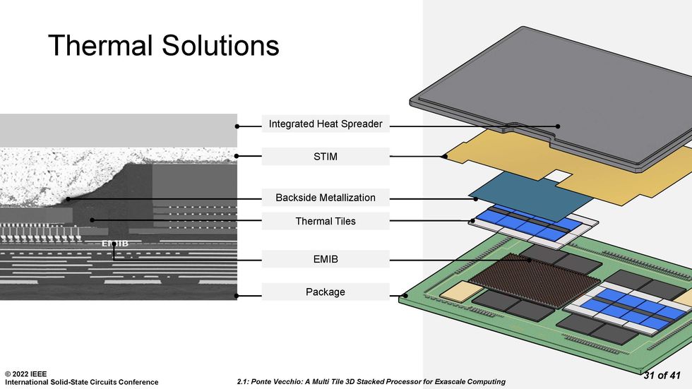
 Getting the heat out of a complex 3D stack of chips was no easy feat.Source: Intel
Ponte Vecchio is meant to consume 600 watts, so making sure heat could be extracted from the 3D stack was always a high priority. Intel engineers used tiles that had no other function than to draw heat away from the active chiplets in the design. They also coated the top of the entire chiplet agglomeration in heat-conducting metal, despite the various parts having different heights. Atop that was a solder-based thermal interface material (STIM), and an integrated heat spreader. The different tiles each have different operating-temperature limits under liquid cooling and air cooling, yet this solution managed to keep them all in range, said Gomes.
"Ponte Vecchio started with a vision that we wanted democratize computing and bring petaflops to the mainstream," said Gomes. Each Ponte Vecchio system is capable of more than 45 trillion 32-bit floating point operations per second (teraflops). Four such systems fit together with two Sapphire Rapids CPUs in a complete compute system. These will be combined for a total exceeding 54,000 Ponte Vecchios and 18,000 Sapphire Rapids to form Aurora, a machine targeting 2 exaflops.
It's taken 14 years to go from the first petaflop supercomputers in 2008—capable of one million billion calculations per second—to exaflops today, Gomes pointed out. A 1000-fold increase in performance "is a really difficult task, and it's taken multiple innovations across many fields," he said. But with improvements in manufacturing processes, packaging, power delivery, memory, thermal control, and processor architecture, Gomes told engineers, the next 1000-fold increase could be accomplished in just six years rather than another 14.
Reference: https://ift.tt/3f2ODrj
No comments:
Post a Comment